


八路边沿触发D型锁存器三态输出 OCTAL EDGE-TRIGGERED D-TYPE LATCHES WITH 3-STATE OUTPUTS
description/ordering information
These 8-bit flip-flops feature 3-state outputs designed specifically for driving highly capacitive or relatively low-impedance loads. They are particularly suitable for implementing buffer registers, I/O ports, bidirectional bus drivers, and working registers.
The eight flip-flops of the ’BCT374 devices are edge-triggered D-type flip-flops. On the positive transition of the clock CLK input, the Q outputs are set to the logic levels that were set up at the data D inputs.
• Operating Voltage Range of 4.5 V to 5.5 V
• State-of-the-Art BiCMOS Design Significantly Reduces ICCZ
• Full Parallel Access for Loading
• Buffered Control Inputs
• 3-State Outputs Drive Bus Lines or Buffer Memory Address Registers
• ESD Protection Exceeds JESD 22
– 2000-V Human-Body Model A114-A
频率 70 MHz
电源电压DC 4.50V ~ 5.50V
输出接口数 8
输出电流 64.0 mA
时钟频率 70 MHz
位数 8
传送延迟时间 10.6 ns
电压波节 5.00 V
输入电容 6 pF
输出电流驱动 -234 µA
输入数 8
工作温度Max 70 ℃
工作温度Min 0 ℃
电源电压 4.5V ~ 5.5V
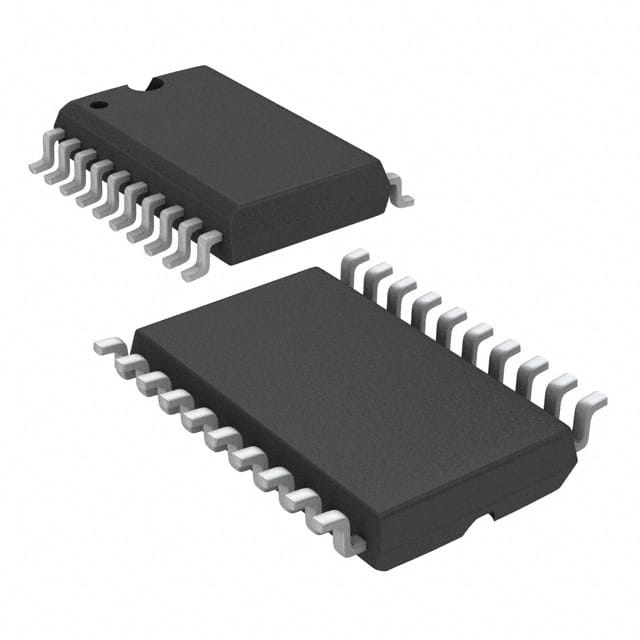
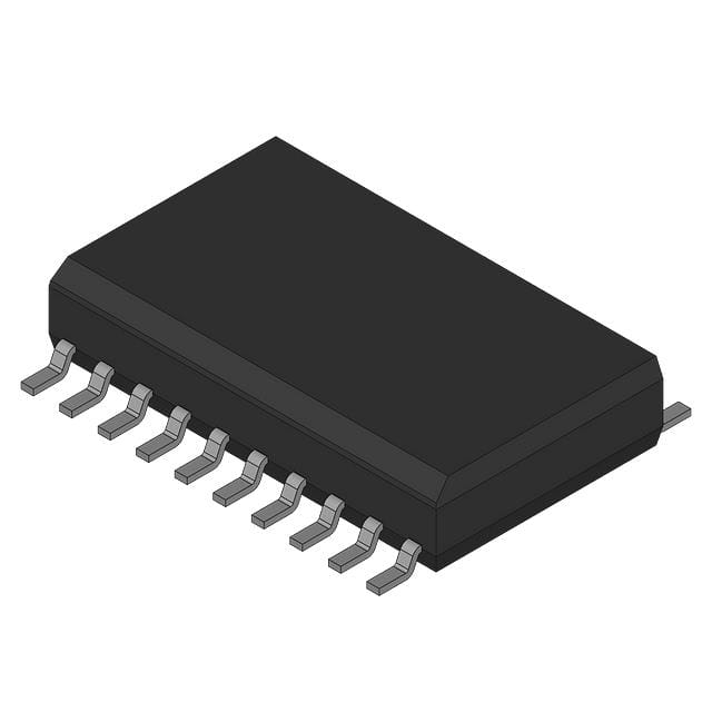
安装方式 Surface Mount
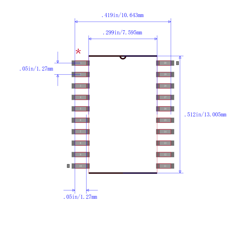
引脚数 20
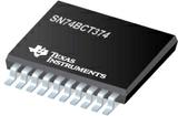
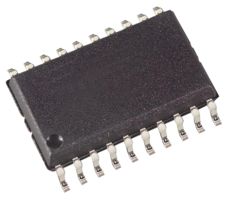
封装 SOIC-20
封装 SOIC-20
工作温度 0℃ ~ 70℃ TA
产品生命周期 Active
包装方式 Tube
RoHS标准 RoHS Compliant
含铅标准 Lead Free
REACH SVHC标准 No SVHC


| 型号/品牌 | 代替类型 | 替代型号对比 |
|---|---|---|
SN74BCT374DW TI 德州仪器 | 当前型号 | 当前型号 |
SN74BCT374DWRG4 德州仪器 | 类似代替 | SN74BCT374DW和SN74BCT374DWRG4的区别 |