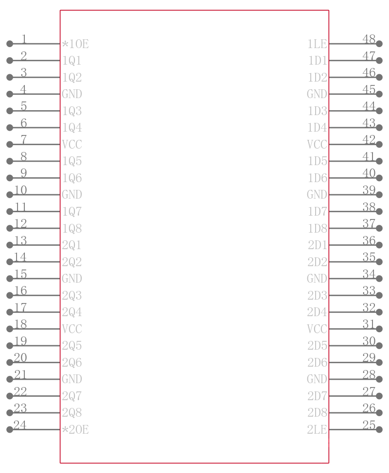


闭锁 16bit Transparent
A Dynamic Output Control DOC circuit is implemented, which, during the transition, initially lowers the output impedance to effectively drive the load and, subsequently, raises the impedance to reduce noise. Figure 1 shows typical VOL vs IOL and VOH vs IOH curves to illustrate the output impedance and drive capability of the circuit. At the beginning of the signal transition, the DOC circuit provides a maximum dynamic drive that is equivalent to a high-drive standard-output device. For more information, refer to the application reports, _AVC Logic Family Technology and Applications_, literature number SCEA006, and _Dynamic Output Control DOC Circuitry Technology and Applications_, literature number SCEA009.
This 16-bit transparent D-type latch is operational at 1.2-V to 3.6-V VCC, but is designed specifically for 1.65-V to 3.6-V VCC operation.
The SN74AVC16373 is particularly suitable for implementing buffer registers, I/O ports, bidirectional bus drivers, and working registers. This device can be used as two 8-bit latches or one 16-bit latch. When the latch-enable LE input is high, the Q outputs follow the data D inputs. When LE is taken low, the Q outputs are latched at the levels set up at the D inputs.
A buffered output-enable OE input can be used to place the eight outputs in either a normal logic state high or low logic levels or the high-impedance state. In the high-impedance state, the outputs neither load nor drive the bus lines significantly. The high-impedance state and the increased drive provide the capability to drive bus lines without need for interface or pullup components. OE does not affect internal operations of the latch. Old data can be retained or new data can be entered while the outputs are in the high-impedance state.
To ensure the high-impedance state during power up or power down, OE should be tied to VCC through a pullup resistor; the minimum value of the resistor is determined by the current-sinking capability of the driver.
This device is fully specified for partial-power-down applications using Ioff. The Ioff circuitry disables the outputs, preventing damaging current backflow through the device when it is powered down.
The SN74AVC16373 is characterized for operation from 40°C to 85°C.
电源电压DC 1.40V ~ 3.60V
输出接口数 16
输出电流 12.0 mA
电路数 2
位数 16
传送延迟时间 3.20 ns
极性 Non-Inverting
电压波节 3.30 V, 2.50 V, 1.80 V, 1.50 V, 1.20 V
输出电流驱动 -1.00 mA
输入数 16
工作温度Max 85 ℃
工作温度Min -40 ℃
电源电压 1.4V ~ 3.6V
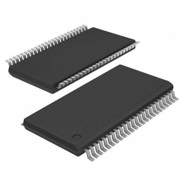
安装方式 Surface Mount
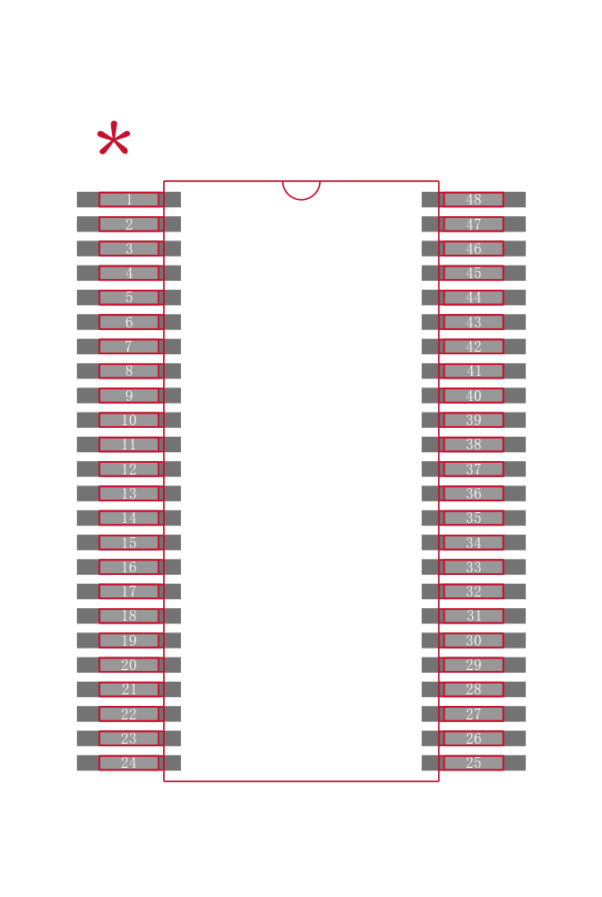
引脚数 48
封装 TVSOP-48
长度 9.7 mm
宽度 4.4 mm
高度 1.05 mm
封装 TVSOP-48
工作温度 -40℃ ~ 85℃
产品生命周期 Active
包装方式 Tape & Reel TR
RoHS标准 RoHS Compliant
含铅标准 Lead Free
ECCN代码 EAR99