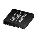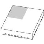


TDA8035HN/C1/S1J 编带
Overview
The TDA8035 is the cost efficient successor of the established integrated contact smart card reader IC TDA8024. It offers a high level of security for the card by performing current limitation, short-circuit detection, ESD protection as well as supply supervision. The current consumption during the standby mode of the contact reader is very low as it operates in the 3 V supply domain. The TDA8035 is therefore the ideal component for a power efficient contact reader.
MoreLess
## Features
### Protection of the contact smart card
* Thermal and short-circuit protection on all card contacts
* VCC regulation:
* 5 V, 3 V, 1.8 V ± 5 % on 2 × 220 nF multilayer ceramic capacitors with low ESR
* current spikes of 40 nA/s VCC = 5 V and 3 V or 15 nA/s VCC = 1.8 V up to 20 MHz, with controlled rise and fall times, filtered overload detection is approximately 120 mA
* Automatic activation and deactivation sequences initiated by software or by hardware in the event of a short-circuit, card take-off, overheating, falling VREG VDDINTF,VDDP
* Enhanced card-side ElectroStatic Discharge ESD protection of > 8 kV
* Supply supervisor for killing spikes during power on and off:
* threshold internally fixed
* externally by a resistor bridge
### Easy integration into your contact reader
* SW compatible to TDA8024 and TDA8034
* 5 V, 3 V, 1.8 V smart card supply
* DC-to-DC converter for VCC generation separately powered from 2.7 V to 5.5 V supply VDDP and GNDP
* Very low power consumption in Deep Shutdown mode
* Three protected half-duplex bidirectional buffered I/O lines C4, C7 and C8
* External clock input up to 26 MHz
* Card clock generation up to 20 MHz using pins CLKDIV1 and CLKDIV2 with synchronous frequency changes of fXTAL, fXTAL/2, fXTAL/4, fXTAL/8
* Non-inverted control of pin RST using pin RSTIN
* Built-in debouncing on card presence contact
* Multiplexed status signal using pin OFFN
* Chip Select digital input for parallel operation of several TDA8035 ICs.
### Other
* HVQFN32 package
* Compliant with ISO 7816, NDS and EMV 4.3 * payment systems
_- .
- for C2 version_
## Target Applications
* Pay TV
* Electronic payment
* Identification
* IC card readers for banking
## Features
| 型号/品牌 | 代替类型 | 替代型号对比 |
|---|---|---|
TDA8035HN/C1/S1J NXP 恩智浦 | 当前型号 | 当前型号 |
TDA8035HN/C1/S1EL 恩智浦 | 完全替代 | TDA8035HN/C1/S1J和TDA8035HN/C1/S1EL的区别 |