
非常低噪声四路运算放大器 Very Low Noise Quad Operational Amplifier
Product Details
The OP470 is a high-performance monolithic quad operational amplifier with exceptionally low voltage noise, 5nV/rootHz at 1kHz Max, offering comparable performance to PMI"s industry standard OP27.
The OP470 features an input offset voltage below 0.4mV, excellent for a quad op amp, and an offset drift under 2µV/°C, guaranteed over the full military temperature range. Open-loop gain of the OP470 is over 1,000,000 into a 10k Ohm load insuring excellent gain accuracy and linearity, even in high-gain applications. Input bias is under 25nA which reduces errors due to signal source resistance. The OP470"s CMR of over 110dB and PSRR of less than 1.8µV/V significantly reduce errors due to ground noise and power supply fluctuations. Power consumption of the quad OP470 is half that of four OP27s, a significant advantage for power conscious applications. The OP470 is unity-gain stable with a gain-bandwidth product of 6MHz and a slew rate of 2V/µs.
The OP470 offers excellent amplifier matching which is important for applications such as multiple gain blocks, low-noise instrumentation amplifiers, quad buffers, and low-noise active filters.
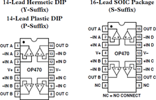
The OP470 conforms to the industry standard 14-pin DIP pinout. It is pin compatible with the OP11, LM 148/149, HA4741, HA5104, and RM4156 quad op amps and can be used to upgrade systems using these devices.
For higher speed applications the OP471, with a slew rate of 8V/µs, is recommended.
### Features and Benefits
- .
- Very Low-Noise, 5 nV/√Hz @ 1 kHz Max
- .
- Excellent Input Offset Voltage, 0.4 mV Max
- .
- Low Offset Voltage Drift, 2 µV/°C Max
- .
- Very High Gain, 1000 V/mV Min
- .
- Outstanding CMR, 110 dB Min
- .
- Slew Rate, 2 V/µs Typ
- .
- Gain-Bandwidth Product, 6 MHz Typ
- .
- Industry Standard Quad Pinouts
- .
- Available in Die Form