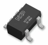


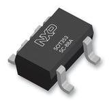

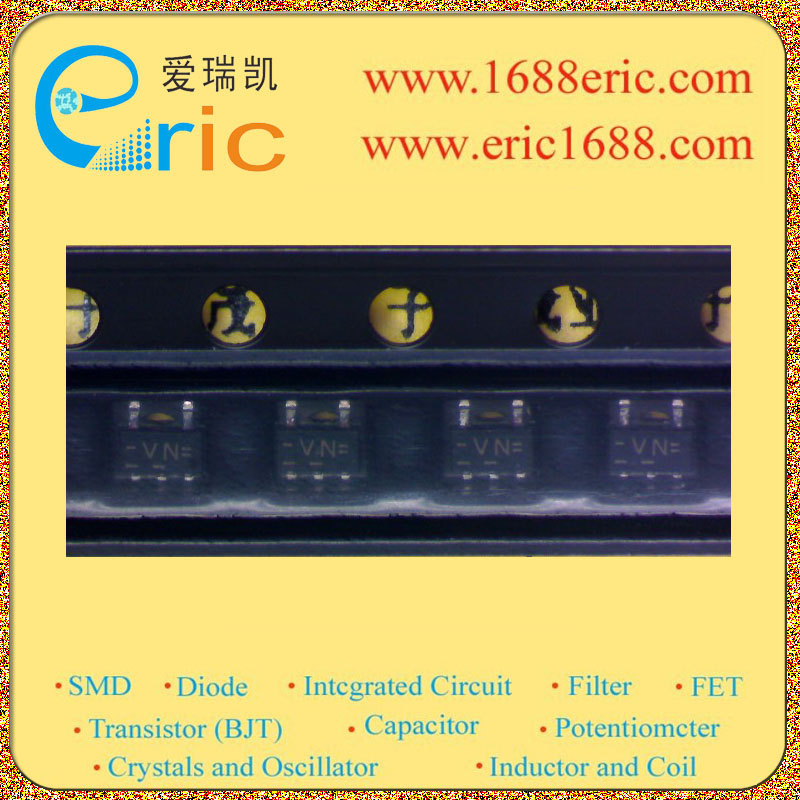
IC 缓存与线路驱动器 74LVC1G126GW SOT-353/SC-88A/TSSOP5 marking/标记 VN
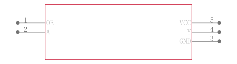
逻辑类型Logic Type| 非反相 Non-Inverting \---|--- 电路数Number of Circuits| 1 输入数Number of Inputs| 1 电源电压VccVoltage - Supply| 1.65 V ~ 5.5 V 静态电流IqCurrent - Quiescent Max| 32mA,32mA 输出高,低电平电流Current - Output High, Low| SINGLE BUS BUFFER GATE AND 5 VOLT TOLERANT I/O;This single bus buffer gate is built using advanced dual metal CMOS technology. features independent line drivers with 3-state outputs. Each output is disabled when the associated output-enable OE input is low. 低逻辑电平Logic Level - Low| 单总线缓冲器闸和5伏宽容的I / O;这种单总线缓冲门是采用先进的双金属CMOS技术。 设有独立的线路驱动器,具有三态输出。 每个输出相关的输出使能(OE)输入为低电平时禁用。 高逻辑电平Logic Level - High| 传播延迟时间@Vcc,CLMax Propagation Delay @ V, Max CL| Description & Applications| 描述与应用|
电源电压DC 1.65V min
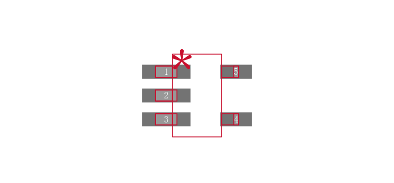
针脚数 5
工作温度Max 125 ℃
工作温度Min -40 ℃
电源电压Max 5.5 V
电源电压Min 1.65 V
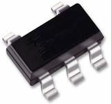
安装方式 Surface Mount
引脚数 5
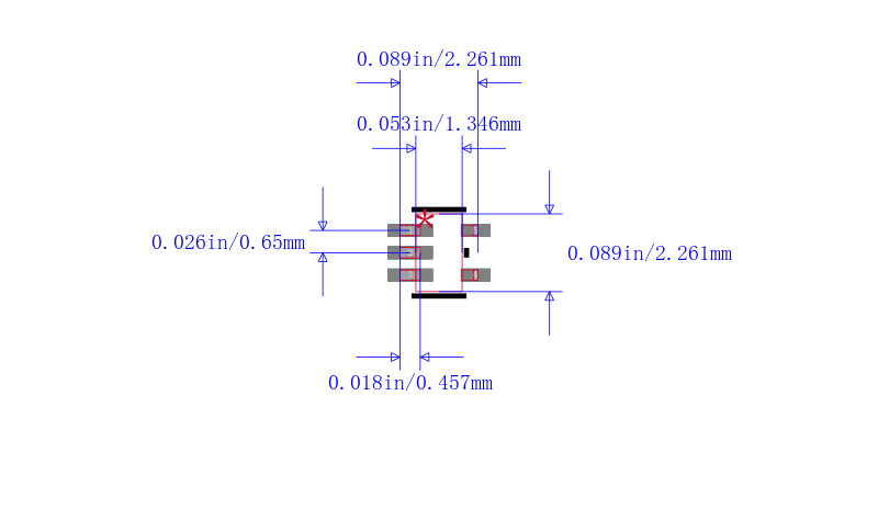
封装 SOT-353
封装 SOT-353
产品生命周期 Unknown
包装方式 Cut Tape CT
制造应用 Industrial, Automation & Process Control, Signal Processing, Automotive
RoHS标准 RoHS Compliant
含铅标准 Lead Free
REACH SVHC标准 No SVHC
REACH SVHC版本 2015/12/17