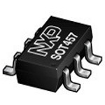

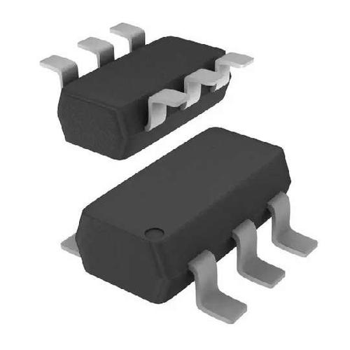
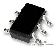
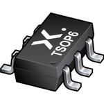
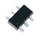


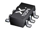

NXP 74LVC1G175GV,125 触发器, 非反相, 正沿, D, 300 MHz, 50 mA, SC-74, 6 引脚
The 74LVC1G175GV is a single positive-edge triggered D-type Flip-flop with individual data D input, clock input, master reset MR\\ input and Q output. The MR\ is an asynchronous active low input and operates independently of the clock input. Information on the data input is transferred to the Q output on the low-to-high transition of the clock pulse. The D input must be stable one set-up time prior to the low-to-high clock transition for predictable operation. The inputs can be driven from either 3.3 or 5V devices. This feature allows the use of this device in a mixed 3.3 and 5V environment. This device is fully specified for partial power-down applications using IOFF. The IOFF circuitry disables the output, preventing the damaging backflow current through the device when it is powered down. Schmitt trigger action at all inputs makes the circuit highly tolerant of slower input rise and fall times.
- .
- High noise immunity
- .
- CMOS low power consumption
- .
- Latch-up performance exceeds 250mA
- .
- Direct interface with TTL levels
- .
- ±24mA Output drive current
频率 300 MHz
电源电压DC 1.65V min
输出接口数 1
输出电流 50 mA
电路数 1
针脚数 6
时钟频率 200 MHz
位数 1
输入电容 2.5 pF
输入数 1
工作温度Max 125 ℃
工作温度Min -40 ℃
电源电压 1.65V ~ 5.5V
电源电压Max 5.5 V
电源电压Min 1.65 V
安装方式 Surface Mount
引脚数 6
封装 SOT-457
宽度 1.7 mm
高度 1 mm
封装 SOT-457
工作温度 -40℃ ~ 125℃ TA
产品生命周期 Active
包装方式 Cut Tape CT
制造应用 Computers & Computer Peripherals, Communications & Networking
RoHS标准 RoHS Compliant
含铅标准 Lead Free
REACH SVHC标准 No SVHC
REACH SVHC版本 2015/12/17