

74LVC1G02GW概述
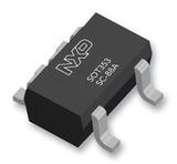
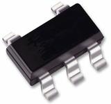
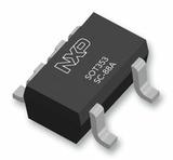
NXP 74LVC1G02GW 或非门, LVC系列, 1门, 2输入, 32 mA, 1.65V至5.5V, SOT-353-5
The is a single 2-input NOR Gate, the input can be driven from either 3.3V or 5V devices. This feature allows the use of this device in a mixed 3.3V and 5V environment. Schmitt-trigger action at all inputs makes the circuit highly tolerant to slower input rise and fall time. This device is fully specified for partial power-down applications using IOFF. The IOFF circuitry disables the output, preventing the damaging backflow current through the device when it is powered down.
- .
- High noise immunity
- .
- Complies with JEDEC standard - JESD8-7, JESD8-5 and JESD8-B/JESD36
- .
- ±24mA Output drive VCC = 3V
- .
- CMOS low power consumption
- .
- Latch-up performance exceeds 250mA
- .
- Direct interface with TTL levels
- .
- Inputs accept voltages up to 5V
- .
- ESD protection - HBM JESD22-A114F exceeds 2000V, MM JESD22-A115-A exceeds 200V
在线购买74LVC1G02GW
型号: 74LVC1G02GW
制造商:
NXP
恩智浦
描述:NXP 74LVC1G02GW 或非门, LVC系列, 1门, 2输入, 32 mA, 1.65V至5.5V, SOT-353-5