
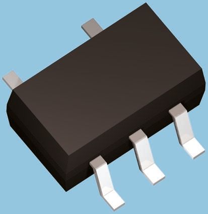
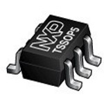
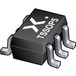
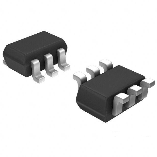
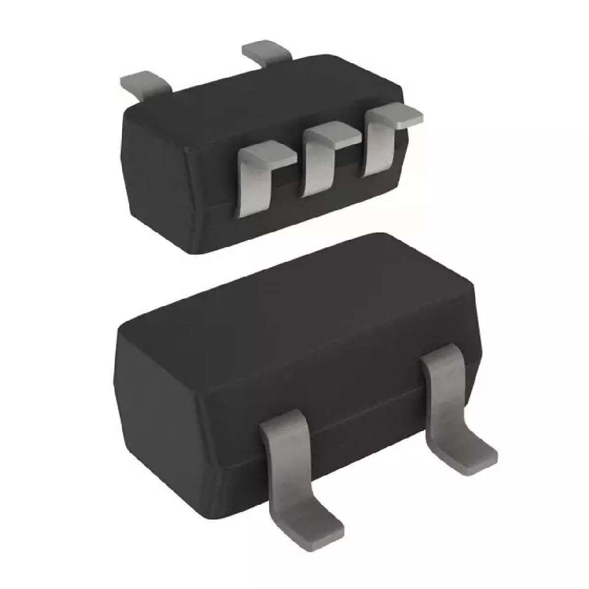
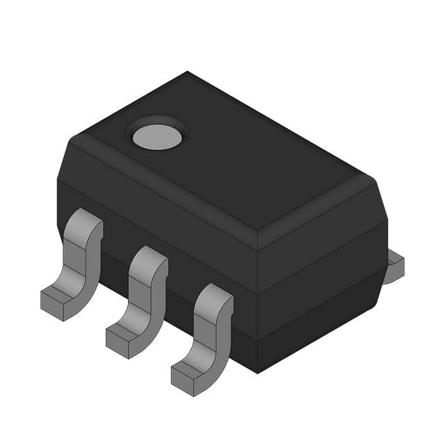
NXP 74LVC1G04GW,125 非门, LVC系列, 超高速, 1输入, 32 mA, 1.65V至5.5V, TSSOP-5
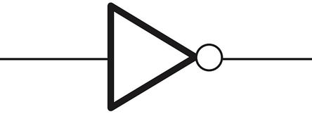
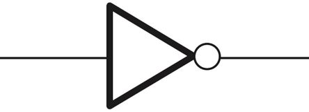
The is a Single Inverter. The 74LVC1G04 provides one inverting buffer. Input can be driven from either 3.3 or 5V devices. This feature allows the use of these devices in a mixed 3.3 and 5V environment. Schmitt-trigger action at all inputs makes the circuit tolerant of slower input rise and fall time. This device is fully specified for partial power-down applications using IOFF. The IOFF circuitry disables the output, preventing the damaging backflow current through the device when it is powered down.
- .
- 5V Tolerant input for interfacing with 5V logic
- .
- High noise immunity
- .
- ±24mA Output drive VCC=3.0V
- .
- CMOS Low power consumption
- .
- Latch-up performance exceeds 250mA
- .
- Direct interface with TTL levels
- .
- Inputs accept voltages up to 5V
- .
- Complies with JEDEC standard
ESD sensitive device, take proper precaution while handling the device.
电源电压DC 1.65V min
输出电流 32 mA
电路数 1
针脚数 5
输入数 1
工作温度Max 125 ℃
工作温度Min -40 ℃
电源电压 1.65V ~ 5.5V
电源电压Max 5.5 V
电源电压Min 1.65 V
安装方式 Surface Mount
引脚数 5
封装 TSSOP-5
长度 2.25 mm
宽度 1.35 mm
高度 1 mm
封装 TSSOP-5
工作温度 -40℃ ~ 125℃
产品生命周期 Active
包装方式 Tape & Reel TR
制造应用 电源管理, Power Management
RoHS标准 RoHS Compliant
含铅标准 Lead Free
REACH SVHC标准 No SVHC
REACH SVHC版本 2015/12/17
ECCN代码 ECL99
香港进出口证 NLR