

NXP 74HC4052PW-Q100,11 芯片, 模拟多路复用器/信号分离器, 双路, 4X1, TSSOP-16
The 74HC4052PW-Q100 is a dual 4-channel Analog Multiplexer/Demultiplexer with common select logic. It is a high-speed Si-gate CMOS device and is pin compatible with Low-power Schottky TTL LSTTL. Each multiplexer has four independent inputs/outputs pins nY0 to nY3 and a common input/output pin nZ. The common channel select logics include two digital select inputs pins S0 and S1 and an active LOW enable input pin E. VCC and GND are the supply voltage pins for the digital control inputs pins S0, S1 and E. The analog inputs/outputs pins nY0 to nY3 and nZ can swing VEE may not exceed between VCC as a positive limit and VEE as a negative limit. For operation as a digital multiplexer/demultiplexer, VEE is connected to GND typically ground.
- .
- Low ON resistance - 80R, 70R, 60R typical at VCC-VEE = 4.5V, 6.0V, 9.0V respectively
- .
- Logic level translation to enable 5V logic to communicate with ±5V analog signals
- .
- Typical break before make built-in
- .
- ESD protection - MIL-STD-833, method 3015 <2000V, HBM JESD22-A114F <2000V, MM JESD22-A115-A <200V
输出接口数 2
供电电流 320 µA
电路数 2
通道数 2
针脚数 16
耗散功率 0.5 W
输入数 8
工作温度Max 125 ℃
工作温度Min -40 ℃
3dB带宽 180 MHz
电源电压 2V ~ 10V
安装方式 Surface Mount
引脚数 16
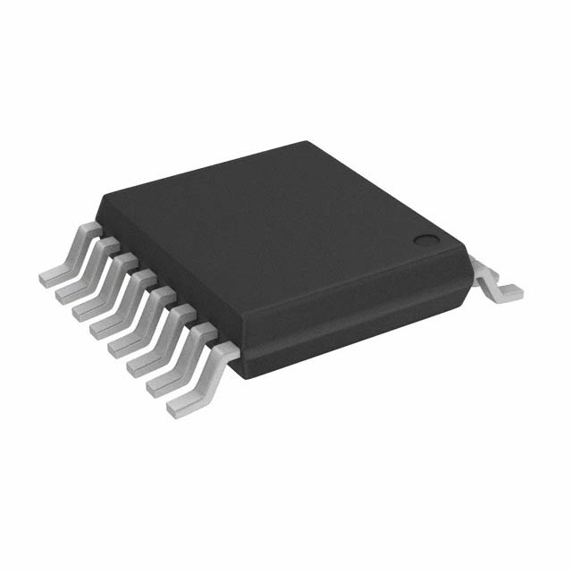
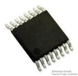
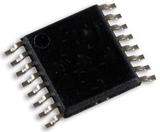
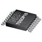
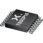
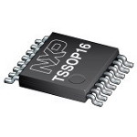
封装 TSSOP-16
封装 TSSOP-16
工作温度 -40℃ ~ 125℃ TA
产品生命周期 Active
包装方式 Cut Tape CT
制造应用 车用, Automotive, Signal Processing, Aerospace, Defence, Military
RoHS标准 RoHS Compliant
含铅标准 Lead Free
REACH SVHC标准 No SVHC
军工级 Yes
REACH SVHC版本 2015/12/17