


低电压与5V容限输入和输出缓冲器/线路驱动器 Low Voltage Buffer/Line Driver with 5V Tolerant Inputs and Outputs
The LCX244 contains eight non-inverting buffers with 3-STATE outputs. The device may be employed as a memory address driver, clock driver and bus-oriented transmitter/receiver. The LCX244 is designed for low voltage 2.5V or 3.3V V
CC
applications with capability of interfacing to a 5V signal environment.
The LCX244 is fabricated with an advanced CMOS technology to achieve high speed operation while maintaining CMOS low power dissipation.
Product Highlights
5V tolerant inputs and outputs
2.3V to 3.6V V
CC
specifications provided
6.5 ns t
PD
max V
CC
= 3.3V, 10 µA I
CC
max
Power down high impedance inputs and outputs
Supports live insertion/withdrawal Note 1
±24 mA output drive V
CC
= 3.0V
Implements patented noise/EMI reduction circuitry
Latch-up performance exceeds 500 mA
ESD performance: Human body model > 2000V Machine model > 200V
Leadless DQFN Pb-Free package
电源电压DC 3.30 V
输出接口数 8
通道数 8
位数 8
输入数 8
工作温度Max 85 ℃
工作温度Min 40 ℃
电源电压 2V ~ 3.6V
电源电压Max 3.6 V
电源电压Min 2 V
安装方式 Surface Mount
引脚数 20
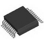
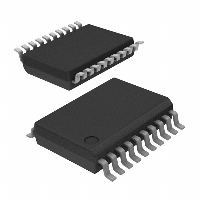
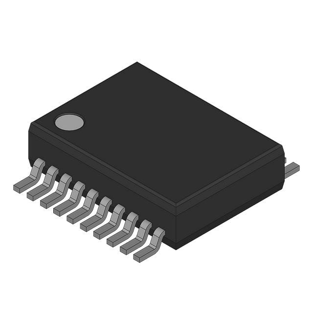
封装 SSOP-20
长度 7.2 mm
宽度 5.3 mm
高度 1.75 mm
封装 SSOP-20
工作温度 -40℃ ~ 85℃ TA
产品生命周期 Obsolete
包装方式 Tape & Reel TR
RoHS标准 RoHS Compliant
含铅标准 Lead Free
ECCN代码 EAR99