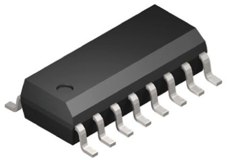
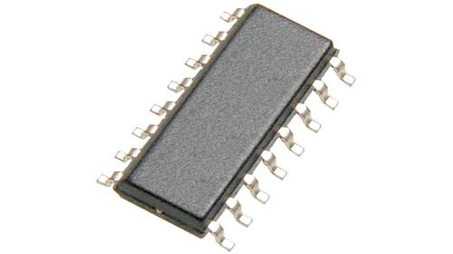
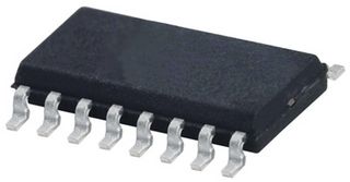
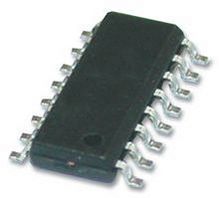
NXP 74HC259D 芯片, 74HC CMOS逻辑器件
The is a 8-bit Addressable Latch features four modes of operation. In the addressable latch mode, data on the D input is written into the latch addressed by the inputs AO to A3. The addressed latch will follow the data input, non-addressed latches will retain their previous states. In memory mode, all latches retain their previous states and are unaffected by the data or address inputs. In the 3-to-8 decoding or demultiplexing mode, the addressed output follows the D input and all other outputs are low. In the reset mode, all outputs are forced low and unaffected by the data or address inputs. Inputs include clamp diodes. This enables the use of current limiting resistors to interface inputs to voltages in excess of VCC.
- .
- Serial-to-parallel capability
- .
- Output from each storage bit available
- .
- Random addressable data entry
- .
- Easily expandable
- .
- Common reset input
- .
- Useful as a 3-to-8 active high decoder
- .
- CMOS Input level
- .
- Complies with JEDEC standard No. 7A
电源电压DC 5.00 V, 6.00 V max
输出电流 25 mA
电路数 1
针脚数 16
位数 8
极性 Non-Inverting
逻辑门个数 1
工作温度Max 125 ℃
工作温度Min -40 ℃
电源电压Max 6 V
电源电压Min 2 V
安装方式 Surface Mount
引脚数 16
封装 SOIC
长度 10 mm
宽度 4 mm
高度 1.45 mm
封装 SOIC
产品生命周期 Unknown
包装方式 Each
制造应用 Consumer Electronics, Industrial
RoHS标准 RoHS Compliant
含铅标准 Lead Free
REACH SVHC标准 No SVHC
REACH SVHC版本 2015/12/17
ECCN代码 EAR99