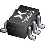


NXP 74LVC1G79GW,125 触发器, 非反相, 正沿, D, 200 MHz, 50 mA, TSSOP, 5 引脚
The 74LVC1G79GW is a single positive-edge triggered D-type Flip-flop features that the information on the data input is transferred to the Q-output on the low-to-high transition of the clock pulse. The D-input must be stable one set-up time prior to the low-to-high clock transition for predictable operation. Inputs can be driven from either 3.3 or 5V devices. This feature allows the use of this device in a mixed 3.3 and 5V environment. This device is fully specified for partial power-down applications using IOFF. The IOFF circuitry disables the output, preventing the damaging backflow current through the device when it is powered down.
- .
- High noise immunity
- .
- CMOS low power consumption
- .
- Latch-up performance exceeds 250mA
- .
- Direct interface with TTL levels
- .
- ±24mA Output drive current
频率 500 MHz
电源电压DC 1.65V min
输出电流 50 mA
电路数 1
针脚数 5
时钟频率 500 MHz
位数 1
输入电容 5 pF
工作温度Max 125 ℃
工作温度Min -40 ℃
电源电压 1.65V ~ 5.5V
电源电压Max 5.5 V
电源电压Min 1.65 V
安装方式 Surface Mount
引脚数 5
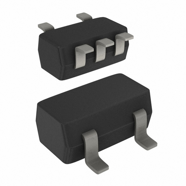
封装 SC-70-5
宽度 1.35 mm
高度 1 mm
封装 SC-70-5
工作温度 -40℃ ~ 125℃ TA
产品生命周期 Active
包装方式 Tape & Reel TR
制造应用 Computers & Computer Peripherals, Communications & Networking
RoHS标准 RoHS Compliant
含铅标准 Lead Free
REACH SVHC标准 No SVHC
REACH SVHC版本 2015/12/17