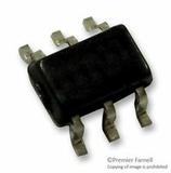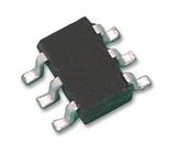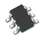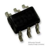


低功耗双缓冲 Low-power dual buffer
The is a low-power low-voltage dual Buffer ensures very low static and dynamic power consumption across the entire VCC range from 0.8 to 3.6V. Schmitt trigger action at all inputs makes the circuit tolerant to slower input rise and fall times across the entire VCC range from 0.8 to 3.6V. This device is fully specified for partial power-down applications using IOFF. The IOFF circuitry disables the output, preventing the damaging backflow current through the device when it is powered down.
- .
- High noise immunity
- .
- IOFF circuitry provides partial power-down mode operation
- .
- Complies with JEDEC standards
- .
- Low static power consumption, ICC = 0.9µA maximum
- .
- Latch-up performance exceeds 100mA per JESD 78 class II
- .
- Inputs accept voltages up to 3.6V
- .
- Low noise overshoot and undershoot <10% of VCC
电源电压DC 800mV min
针脚数 6
工作温度Max 125 ℃
工作温度Min -40 ℃
电源电压Max 3.6 V
电源电压Min 0.8 V
安装方式 Surface Mount
引脚数 6
封装 SOT-363
封装 SOT-363
工作温度 -40℃ ~ 125℃
产品生命周期 Unknown
包装方式 Each
制造应用 Industrial, Signal Processing, Automation & Process Control
RoHS标准 RoHS Compliant
REACH SVHC标准 No SVHC
REACH SVHC版本 2015/12/17