


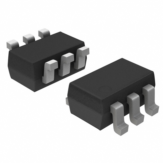
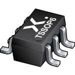
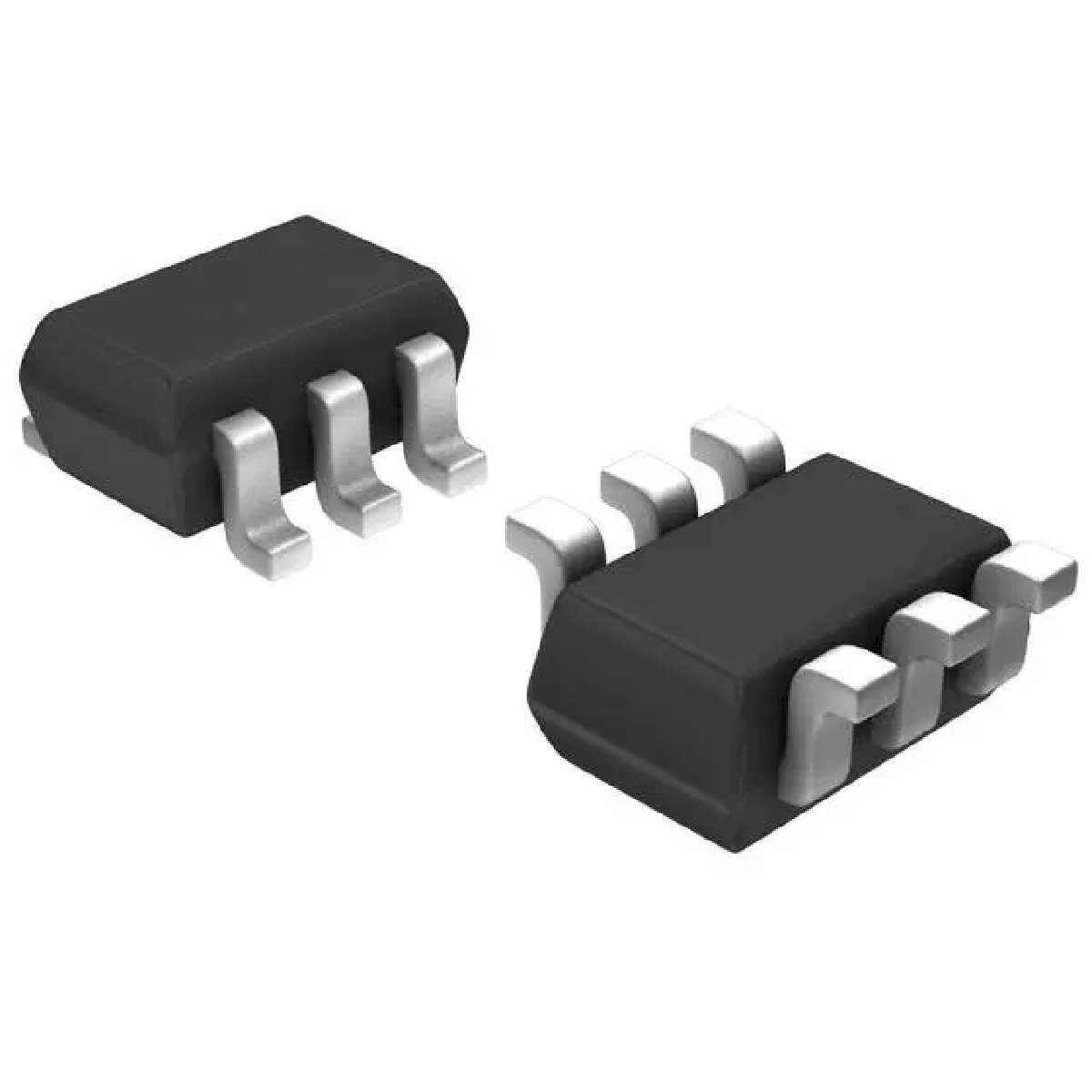
AND Gate 1Element 3IN CMOS 6Pin TSSOP T/R
The 74LVC1G11GW is a single 3-input AND Gate, the input can be driven from either 3.3V or 5V devices. This feature allows the use of this device in a mixed 3.3V and 5V environment. Schmitt-trigger action at all inputs makes the circuit highly tolerant to slower input rise and fall time. This device is fully specified for partial power-down applications using IOFF. The IOFF circuitry disables the output, preventing the damaging backflow current through the device when it is powered down.
- .
- 5V Tolerant inputs for interfacing with 5V logic
- .
- High noise immunity
- .
- Complies with JEDEC standard - JESD8-7, JESD8-5 and JESD8-B/JESD36
- .
- ±24mA Output drive VCC = 3V
- .
- ESD protection - HBM JESD22-A114F exceeds 2000V, MM JESD22-A115-A exceeds 200V
- .
- CMOS low power consumption
- .
- Latch-up performance exceeds 250mA
- .
- Direct interface with TTL levels
电源电压DC 1.65V min
输出接口数 1
输出电流 50 mA
电路数 1
针脚数 6
输入数 3
工作温度Max 125 ℃
工作温度Min -40 ℃
电源电压 1.65V ~ 5.5V
电源电压Max 5.5 V
电源电压Min 1.65 V
安装方式 Surface Mount
引脚数 6
封装 TSSOP-6
高度 1 mm
封装 TSSOP-6
工作温度 -40℃ ~ 125℃
产品生命周期 Active
包装方式 Tape & Reel TR
制造应用 Industrial
RoHS标准 RoHS Compliant
含铅标准 Lead Free
REACH SVHC标准 No SVHC
REACH SVHC版本 2015/12/17