

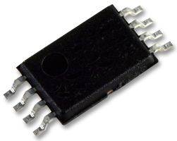

NXP 74LVC1G53DP,125 芯片, 模拟多路复用器/信号分离器, 单路, 2X1, TSSOP-8
The 74LVC1G53DP is an Analog Multiplexer/Demultiplexer with a digital select input S, two independent inputs/outputs Y0 and Y1, a common input/output Z and an active low enable input E. When pin E is HIGH, the switch is turned off. Schmitt trigger action at the select and enable inputs makes the circuit tolerant of slower input rise and fall times across the entire VCC range from 1.65 to 5.5V. The 74LVC1G53 is a low-power, low-voltage, high-speed, Si-gate CMOS device.
- .
- Very low ON resistance - 7.5R, 6.5R, 6R typical at VCC = 2.7V, 3.3V, 5V respectively
- .
- Switch current capability of 32mA
- .
- High noise immunity
- .
- CMOS low power consumption
- .
- TTL interface compatibility at 3.3V
- .
- Latch-up performance meets requirements of JESD 78 Class I
- .
- ESD protection - HBM JESD22-A114F <2000V, MM JESD22-A115-A <200V, CDM JESD22-C101E <1000V
- .
- Control inputs accept voltages up to 5V
输出接口数 1
供电电流 40 µA
电路数 1
通道数 1
针脚数 8
耗散功率 0.25 W
输入数 2
工作温度Max 125 ℃
工作温度Min -40 ℃
3dB带宽 300 MHz
耗散功率Max 250 mW
电源电压 1.65V ~ 5.5V
安装方式 Surface Mount
引脚数 8
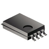
封装 TSSOP-8
封装 TSSOP-8
工作温度 -40℃ ~ 125℃
产品生命周期 Active
包装方式 Cut Tape CT
制造应用 Signal Processing
RoHS标准 RoHS Compliant
含铅标准 Lead Free
REACH SVHC标准 No SVHC
REACH SVHC版本 2015/12/17