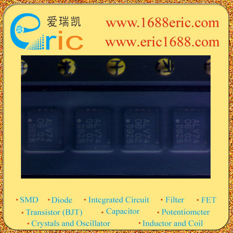
IC 上升沿触发器 74ALVC74BQ DHVQFN14 marking/标记 ALV74
逻辑类型Logic Type| 设置(预设)和复位 SetPreset and Reset \---|--- 电路数Number of Circuits| D型 D-Type 输入数Number of Inputs| 差分 Differential 电源电压VccVoltage - Supply| 2 静态电流IqCurrent - Quiescent Max| 1 输出高,低电平电流Current - Output High, Low| 275MHz 低逻辑电平Logic Level - Low| 3.7ns 高逻辑电平Logic Level - High| 正边沿 Positive Edge 传播延迟时间@Vcc,CLMax Propagation Delay @ V, Max CL| 24mA,24mA Description & Applications| 1.65 V ~ 3.6 V 描述与应用| Dual D-type flip-flop with set and reset;positive-edge trigger DESCRIPTION The 74ALVC74 is a dual positive-edge triggered, D-type flip-flop with individual data D, clock CP, set SD and reset RD inputs and complementary Q and Q outputs. The set and reset are asynchronous active LOW inputs and operate independently of the clock input. Information on the data input is transferred to the Q output on the LOW-to-HIGH transition of the clock pulse. The D inputs must be stable one set-up time prior to the LOW-to-HIGH clock transition for predictable operation. Schmitt-trigger action in the clock input makes the circuit highly tolerant to slower clock rise and fall times. FEATURES • Wide supply voltage range from 1.65 to 3.6 V • Complies with JEDEC standard: JESD8-7 1.65 to 1.95 V JESD8-5 2.3 to 2.7 V JESD8B/JESD36 2.7 to 3.6 V. • 3.6 V tolerant inputs/outputs • CMOS low power consumption • Direct interface with TTL levels 2.7 to 3.6 V • Power-down mode • Latch-up performance exceeds 250 mA • ESD protection: HBM EIA/JESD22-A114-A exceeds 2000 V MM EIA/JESD22-A115-A exceeds 200 V.
封装 DHVQFN-14
封装 DHVQFN-14
逻辑类型Logic Type 设置(预设)和复位 SetPreset and Reset
电路数Number of Circuits D型 D-Type
输入数Number of Inputs 差分 Differential
电源电压VccVoltage - Supply 2
静态电流IqCurrent - Quiescent Max 1
输出高,低电平电流Current - Output High, Low 275MHz
低逻辑电平Logic Level - Low 3.7ns
高逻辑电平Logic Level - High 正边沿 Positive Edge
传播延迟时间@Vcc,CLMax Propagation Delay @ V, Max CL 24mA,24mA
规格书PDF __
RoHS标准 RoHS Compliant