


时钟驱动器及分配 BBG ECL PECL CLOCK DRVR
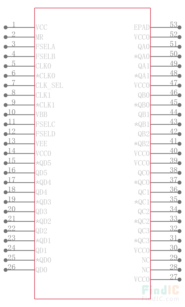
The NB100LVEP222 is a low skew 2:1:15 differential div 1/div 2 ECL fanout buffer designed with clock distribution in mind. The LVECL/LVPECL input signal pairs can be used in a differential configuration or single-ended with VBB output reference bypassed and connected to the unused input of a pair. Either of two fully differential clock inputs may be selected. Each of the four output banks of 2, 3, 4, and 6 differential pairs may be independently configured to fanout 1X or 1/2X of the input frequency. When the output banks are configured with the div 1 mode, data can also be distributed. The LVEP222 specifically guarantees low output to output skew. Optimal design, layout, and processing minimize skew within a device and from lot to lot. This device is an improved version of the MC100LVE222 with higher speed capability and reduced skew. The fsel pins and CLK_Sel pin are asynchronous control inputs. Any changes may cause indeterminate output states requiring an MR pulse to resynchronize any 1/2X outputs See Figure 4. Unused output pairs should be left unterminated open to reduce power and switching noise. The NB100LVEP222, as with most ECL devices, can be operated from a positive VCC/VCC0 supply in LVPECL mode. This allows the LVEP222 to be used for high performance clock distribution in 2.5/3.3 V systems. In a PECL environment series or Thevenin line, terminations are typically used as they require no additional power supplies. For more information on using PECL, designers should refer to Application Note AN1406/D. For a SPICE model, refer to Application Note AN1560/D. The VBB pin, an internally generated voltage supply, is available to this device only. For single-ended LVPECL input conditions, the unused differential input is connected to VBB as a switching reference voltage. VBB may also rebias AC coupled inputs. When used, decouple VBB and VCC/VCC0 via a 0.01 uF capacitor and limit current sourcing or sinking to 0.5 mA. When not used, VBB should be left open
Features
---
|
- .
- 20 ps Output-to-Output Skew
- .
- 85 ps Part-to-Part Skew
- .
- Selectable 1x or 1/2x Frequency Outputs
- .
- LVPECL Mode Operating Range: VCC= 2.375 V to 3.8 V with VEE = 0 V
- .
- NECL Mode Operating Range: VCC = 0 V with VEE = -2.375 V to -3.8 V
- .
- Internal Input Pulldown Resistors
- .
- Performance Upgrade to "s MC100LVE222
- .
- VBB Output
无卤素状态 Halogen Free
输出接口数 15
电路数 1
占空比 50.5 %
最大占空比 50.5 %
工作温度Max 85 ℃
工作温度Min -40 ℃
电源电压 2.375V ~ 3.8V
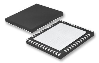
安装方式 Surface Mount
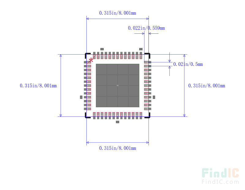
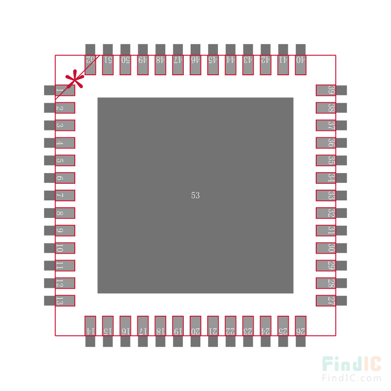
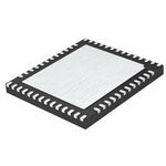
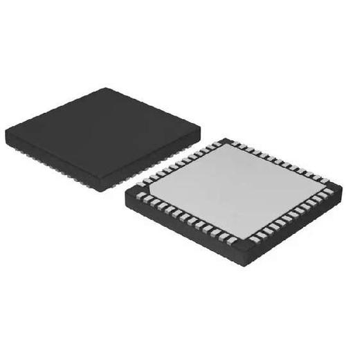
引脚数 52
封装 QFN-52
长度 8 mm
宽度 8 mm
高度 1 mm
封装 QFN-52
工作温度 -40℃ ~ 85℃
产品生命周期 Active
包装方式 Tray
制造应用 Clock Distribution
RoHS标准 RoHS Compliant
含铅标准 Lead Free
ECCN代码 EAR99