
低边 MOSFET 灌:5A 拉:5A
Description:
The input signals are low voltage TTL and 3.3V CMOS-compatible with a very broad voltage handling capability of up to +20V and down to -10VDC. The unique ability to handle -10VDC at the input pins protects the device against ground bouncing. Each of the two outputs is able to sink and source a 5A current utilizing a true rail-to-rail output stage, which ensures very low impedances of 0.7Ω up to the positive and 0.55Ω down to the negative
rail respectively.
Excellent channel to channel delay matching, typ. 1ns, enables risk-free doubling of the source and sink capability up to 10A peak through paralleling of both channels. The combination of industry standard pin-outs and different logic input/output configurations guarantee high flexibility and shortens R&D time. The gate driver is available in the three package options: PG-DSO-8-pin, PG-VDSON-8-pin and PG-TDSSO-8-pin small form-factor, improved thermal performance compared to DSO-8.
Summary of Features:
- .
- 5A peak source/sink current
- .
- 5ns typ. rise/fall times
- .
- < 10ns propagation delay tolerance
- .
- 8V UVLO option
- .
- 19 ns typ. propagation delay for both, for control inputs and for enable
- .
- -10V control and enable input
robustness
- .
- Outputs robust against reverse current
- .
- 2 independent channels
- .
- < 1ns channel-to-channel miss-match
- .
- Industry standard pin-out and packages
Benefits:
- .
- Fast Miller plateau transition
- .
- Precise timing
- .
- Fast and reliable MOSFET turn-off, independent of control IC
- .
- Increased GND-bounce robustness
- .
- Saves switching diodes
- .
- Option to increase drive current by truly concurrent switching of 2 channels
- .
- Straight-forward design up-grades
上升/下降时间 5.3ns, 4.5ns
输出接口数 2
输出电流 5 A
上升时间 5.3 ns
下降时间 4.5 ns
下降时间Max 4.5 ns
上升时间Max 5.3 ns
工作温度Max 150 ℃
工作温度Min 40 ℃
电源电压 4.5V ~ 20V
电源电压Max 20 V
电源电压Min 4.5 V
安装方式 Surface Mount
引脚数 8
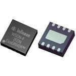
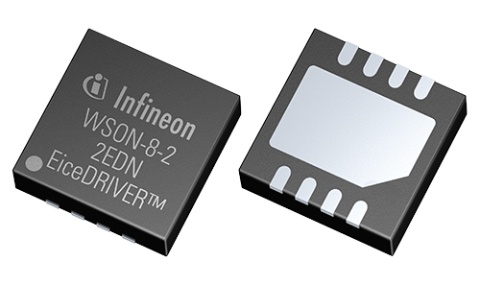
封装 PG-WSON-8-1
封装 PG-WSON-8-1
工作温度 -40℃ ~ 150℃ TJ
产品生命周期 Active
包装方式 Tape & Reel TR
制造应用 DC-DC converters
RoHS标准 RoHS Compliant
含铅标准 Lead Free
ECCN代码 EAR99