
Octal Channel Octal ADC Delta-Sigma 16KSPS 24Bit Serial 64Pin LFCSP EP T/R
Product Details
The AD7779 is an 8-channel, simultaneous sampling ADC. There are eight full Σ-Δ ADCs on chip. The AD7779 provides an ultralow input current to allow direct sensor connection. Each input channel has a programmable gain stage allowing gains of 1, 2, 4, and 8 to map lower amplitude sensor outputs into the full-scale ADC input range, maximizing the dynamic range of the signal chain. The AD7779 accepts VREF from 1 V up to 3.6 V. The analog inputs accept unipolar 0 V to VREF/GAIN or true bipolar ±VREF/GAIN/2 V analog input signals with 3.3 V or ±1.65 V analog supply voltages. The analog inputs can be configured to accept true differential, pseudo differential, or singleended signals to match different sensor output configurations.
Each channel contains an ADC modulator and a sinc3, low latency digital filter. An SRC is provided to allow fine resolution control over the AD7779 ODR. This control can be used in applications where the ODR resolution is required to maintain coherency with 0.01 Hz changes in the line frequency. The SRC is programmable through the serial port interface SPI. The AD7779 implements two different interfaces: a data output interface and SPI control interface. The ADC data output interface is dedicated to transmitting the ADC conversion results from the AD7779 to the processor. The SPI interface is used to write to and read from the AD7779 configuration registers and for the control and reading of data from the SAR ADC. The SPI interface can also be configured to output the Σ-Δ conversion data.
The AD7779 includes a 12-bit SAR ADC. This ADC can be used for AD7779 diagnostics without having to decommission one of the Σ-Δ ADC channels dedicated to system measurement functions. With the use of an external multiplexer, which can be controlled through the three general-purpose inputs/outputs pins GPIOs, and signal conditioning, the SAR ADC can be used to validate the Σ-Δ ADC measurements in applications where functional safety is required. In addition, the AD7779 SAR ADC includes an internal multiplexer to sense internal nodes.
The AD7779 contains a 2.5 V reference and reference buffer. The reference has a typical temperature coefficient of 10 ppm/°C. The AD7779 offers two modes of operation: high resolution mode and low power mode. High resolution mode provides a higher dynamic range while consuming 10.75 mW per channel; low power mode consumes just 3.37 mW per channel at a reduced dynamic range specification.
The specified operating temperature range is −40°C to +105°C, although the device is operational up to +125°C.
**Applications**
- .
- Circuit breakers
- .
- General-purpose data acquisition
- .
- Electroencephalography EEG
- .
- Industrial process control
### Features and Benefits
- .
- 8-channel, 24-bit simultaneous sampling analog-to-digital converter ADC
- .
- Single-ended or true differential inputs
- .
- Programmable gain amplifier PGA per channel gains of 1, 2, 4, and 8
- .
- Low dc input current
- .
- ±1.5 nA differential
- .
- ±4 nA single-ended
- .
- Up to 16 kSPS output data rate ODR per channel
- .
- Programmable ODRs and bandwidth
- .
- Sample rate converter SRC for coherent sampling
- .
- Sampling rate resolution up to 15.2 µSPS
- .
- Low latency sinc3 filter path
- .
- Adjustable phase synchronization
- .
- Internal 2.5 V reference
- .
- Two power modes optimizing power dissipation and performance: high resolution mode and low power mode
- .
- Low resolution successive approximation SAR ADC for system and chip diagnostics
- .
- Power supply
- .
- Bipolar ±1.65 V or unipolar 3.3 V supplies
- .
- Digital input/output I/O supply: 1.8 V to 3.6 V
- .
- Performance temperature range: –40°C to +105°C
- .
- Functional temperature range: –40°C to +125°C
- .
- Performance
- .
- Combined ac and dc performance
- .
- 108 dB signal-to-noise ratio SNR/dynamic range at 16 kSPS in high resolution mode
- .
- −109 dB total harmonic distortion THD
- .
- ±7 ppm integral nonlinearity INL
- .
- ±40 µV offset error
- .
- ±0.1% gain error±10 ppm/°C typical temperature coefficient
- .
- ±10 ppm/°C typical temperature coefficient
耗散功率 86 mW
模数转换数ADC 8
工作温度Max 105 ℃
工作温度Min -40 ℃
耗散功率Max 133 mW
输入通道数 8
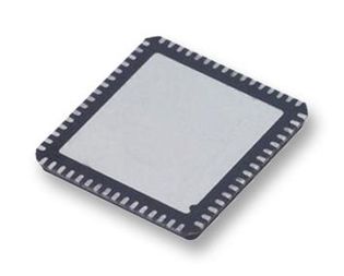
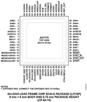
引脚数 64
封装 LFCSP EP
封装 LFCSP EP
工作温度 -40℃ ~ 125℃
产品生命周期 Active
包装方式 Tape & Reel TR
制造应用 Healthcare, Spectrometer, ECG Patient Monitoring, Life Sciences & Medical Instrumentation, Clinical Monitoring
RoHS标准 RoHS Compliant
含铅标准 Lead Free
| 型号/品牌 | 代替类型 | 替代型号对比 |
|---|---|---|
AD7779ACPZ-RL ADI 亚德诺 | 当前型号 | 当前型号 |
AD7779ACPZ 亚德诺 | 功能相似 | AD7779ACPZ-RL和AD7779ACPZ的区别 |