
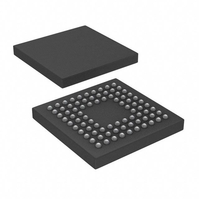
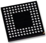


ANALOG DEVICES ADUCM322BBCZ 微控制器, 32位, ARM 皮质-M3, 80 MHz, 256 KB, 32 KB, 96 引脚, CSPBGA 新
Product Details
The ADuCM322 is a fully integrated, single package device that incorporates high performance analog peripherals together with digital peripherals controlled by an 80 MHz ARM® Cortex™-M3 processor and integral flash for code and data.
The ADC on the ADuCM322 provides 12-bit, 1 MSPS data acquisition on up to 16 input balls. Additionally, chip temperature and supply voltages can be measured.
The ADC input voltage range is 0 V to VREF. A sequencer is provided, which allows a user to select a set of ADC channels to measure in sequence without software involvement during the sequence. The sequence can optionally repeat automatically at a user selectable rate. Up to eight VDACs are provided with output ranges that are programmable to one of two voltage ranges.
The ADuCM322 can be configured so that the digital and analog outputs retain their output voltages through a watchdog or software reset sequence. Thus, a product can remain functional even while the ADuCM322 is resetting itself.
The ADuCM322 has a low power ARM Cortex-M3 processor and a 32-bit RISC machine that offers up to 100 MIPS peak perfor-mance. Also integrated on-chip are 2 × 128 kB Flash/EE memory blocks and 32 kB of SRAM. The flash comprises two separate 128 kB blocks supporting execution from one flash block and simultaneous writing/erasing of the other flash block.
The ADuCM322 operates from an on-chip oscillator or a 16 MHz external crystal and a PLL at 80 MHz. This clock can optionally be divided down to reduce current consumption. Additional low power modes can be set via software. In normal operating mode, the ADuCM322 digital core consumes about 300 μA per MHz.
The device includes an MDIO interface capable of operating at up to 4 MHz. The capability to simultaneously execute from one flash block and write/erase the other flash block makes the ADuCM322 ideal for 10G, 40G, and 100G optical applications. In addition, the nonerasable kernel code plus flags in user flash provide assistance by allowing user code to robustly switch between the two blocks of user flash code and data spaces.
The ADuCM322 integrates a range of on-chip peripherals that can be configured under software control, as required in the application. These peripherals include 1 × UART, 2 × I2C, and 2 × SPI serial input/output communication controllers, GPIO, 32-element PLA, three general-purpose timers, plus a wake-up timer and system watchdog timer. A 16-bit PWM with seven output channels is also provided.
GPIO balls on the device power up in high impedance input mode. In output mode, the software chooses between open-drain mode and push-pull mode. The pull-up resistors can be disabled and enabled in software. In GPIO output mode, the inputs can remain enabled to monitor the balls. The GPIO balls can also be programmed to handle digital or analog peripheral signals; in such cases, the ball characteristics are matched to the specific requirement.
A large support ecosystem is available for the ARM Cortex-M3 processor to ease product development of the ADuCM322. Access is via the ARM serial wire debug port SW-DP. On-chip factory firmware supports in-circuit serial download via MDIO. These features are incorporated into a QuickStart™ development system, supporting this precision analog microcontroller family.
Applications
- .
- Optical networking
### Features and Benefits
Analog input/output
- .
- Multichannel, 12-bit, 1 MSPS analog-to-digital converter ADC
- .
- Up to 16 ADC input channels
- .
- 8 x 12-bit VDACs with a range of 0 V to 2.5 V or AVDD
- .
- Voltage comparator
Microcontroller
- .
- ARM Cortex-M3 processor, 32-bit RISC architecture
Clocking options
- .
- 80 MHz PLL with programmable divider
- .
- Trimmed on-chip oscillator ±3%
Memory
- .
- 2 × 128 kB independent Flash/EE memories
- .
- 10,000 cycle Flash/EE endurance
- .
- 20-year Flash/EE retention
- .
- 32 kB SRAM
On-chip peripherals
- .
- MDIO slave up to 4 MHz
- .
- 2 × I2C, 2 × SPI, UART
Temperature range
- .
- Fully specified for −40°C to +105°C ambient operation
See data sheet for additional features.
频率 80 MHz
针脚数 96
时钟频率 80.0 MHz
RAM大小 32 KB
位数 32
耗散功率 1000 mW
模数转换数ADC 1
工作温度Max 105 ℃
工作温度Min -40 ℃
耗散功率Max 1000 mW
数模转换数DAC 1
电源电压Max 3.6 V
电源电压Min 2.9 V
引脚数 96
封装 CSP-BGA
封装 CSP-BGA
工作温度 -40℃ ~ 105℃
产品生命周期 Active
包装方式 Each
RoHS标准 RoHS Compliant
含铅标准 无铅
REACH SVHC版本 2015/12/17
ECCN代码 3A991.a.2
| 型号/品牌 | 代替类型 | 替代型号对比 |
|---|---|---|
ADUCM322BBCZ ADI 亚德诺 | 当前型号 | 当前型号 |
ADUCM322BBCZ-RL 亚德诺 | 功能相似 | ADUCM322BBCZ和ADUCM322BBCZ-RL的区别 |