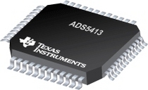

低功耗模数转换器
The is a low power, 12-bit, 65-MSPS, CMOS pipeline analog-to-digital converter ADC that operates from a single 3.3-V supply, while offering the choice of digital output levels from 1.8 V to 3.3 V. The low noise, high linearity, and low clock jitter makes the ADC well suited for high-input frequency sampling applications. On-chip duty cycle adjust circuit allows the use of a non-50% duty cycle. This can be bypassed for applications requiring low jitter or asynchronous sampling. The device can also be clocked with single ended or differential clock, without change in performance. The internal reference can be bypassed to use an external reference to suit the accuracy and low drift requirements of the application.
The device is specified over full temperature range 40°C to +85°C.
- .
- 12-Bit Resolution
- .
- 65-MSPS Maximum Sample Rate
- .
- 2-Vpp Differential Input Range
- .
- 3.3-V Single Supply Operation
- .
- 1.8-V to 3.3-V Output Supply
- .
- 400-mW Total Power Dissipation
- .
- Twos Complement Output Format
- .
- On-Chip S/H and Duty Cycle Adjust Circuit
- .
- Internal or External Reference
- .
- 48-Pin TQFP Package With PowerPad
7 mm x 7 mm body size
- .
- 64.5-dBFS SNR and 72-dBc SFDR at 65 MSPS and 190-MHz Input
- .
- Power-Down Mode
- .
- Single-Ended or Differential Clock
- .
- 1-GHz -3-dB Input Bandwidth
- .
- APPLICA ONS
- .
- High IF Sampling Receivers
- .
- Medical Imaging
- .
- Portable Instrumentation
CommsADC is a trademark of Texas Instruments.