降压型 Vin=2.75V~6V Vout=500mV~4.5V 1A 2A 2A 4A
Product Details
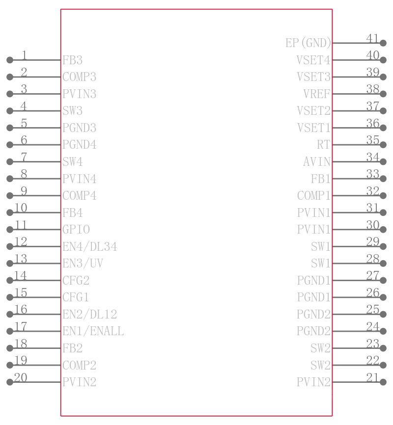
The ADP5014 combines four high performance, low noise buck regulators in a 40-lead LFCSP package. Relying on its low output noise ~25 μV rms when VOUT ≤ VREF, the low noise buck regulator enables the powering up of the noise sensitive signal chain products.
All channels in the ADP5014 integrate high-side and low-side power metal-oxide semiconductor field effect transistors MOSFET. Channel 1 and Channel 2 deliver a programmable output current of 2 A or 4 A. Combining Channel 1 and Channel 2 in a parallel configuration provides a single output with up to 8 A of current.
Channel 3 and Channel 4 deliver a programmable output current of 1 A and 2 A. Combining Channel 3 and Channel 4 in a parallel configuration can provide a single output with up to 4 A of current.
The ADP5014 features two enable modes. The manual mode has four individual precision enable pins to enable each regulator manually. Alternatively, the sequence mode has one grouped precision enable signal with programmable power-up and power-down delay timers on each rail for specific rail sequence requirements.
The switching frequency of the ADP5014 can be programmed or synchronized to an external clock from 500 kHz to 2.5 MHz.
The ADP5014 offers other key features like selective forced pulse width modulation FPWM/power saving mode PSM, an undervoltage output UVO, active output discharge, and a power-good flag. Other safety features include input under-voltage lockout UVLO, overvoltage protection OVP, overcurrent protection OCP and thermal shutdown TSD.
**Applications**
- .
- RF transceiver, high speed analog-to-digital converter ADC/digital-to-analog converter DAC, mixed signal ASIC
- .
- Field programmable gate array FPGA and processor applications
- .
- Security and surveillance
- .
- Medical applications
### Features and Benefits
- .
- Input voltage range: 2.75 V to 6.0 V
- .
- Programmable output voltage range: 0.5 V to 0.9 × PVINx
- .
- Low output noise: ~25 μV rms when VOUT ≤ VREF
- .
- ±1.0% output accuracy over full temperature range
- .
- 500 kHz to 2.5 MHz adjustable switching frequency
- .
- Power regulation
- .
- Channel 1 and Channel 2: programmable 2 A/4 A sync buck regulators, or single 8 A output in parallel
- .
- Channel 3 and Channel 4: programmable 1 A/2 A sync buck regulators, or single 4 A output in parallel
- .
- Flexible parallel operation
- .
- Precision enable with 0.6 V threshold
- .
- Manual or sequence mode for power-up and power-down sequence
- .
- Selective FPWM or PSM operation mode
- .
- Precision undervoltage comparator
- .
- Frequency synchronization input or output
- .
- Active output discharge switch
- .
- Power-good flag on selective channels via factory fuse
- .
- UVLO, OVP, OCP, and TSD protection
- .
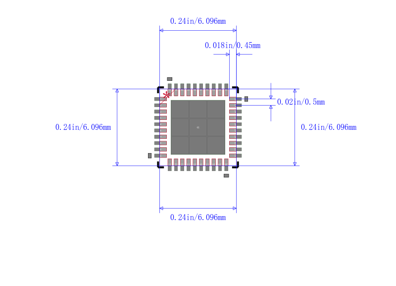
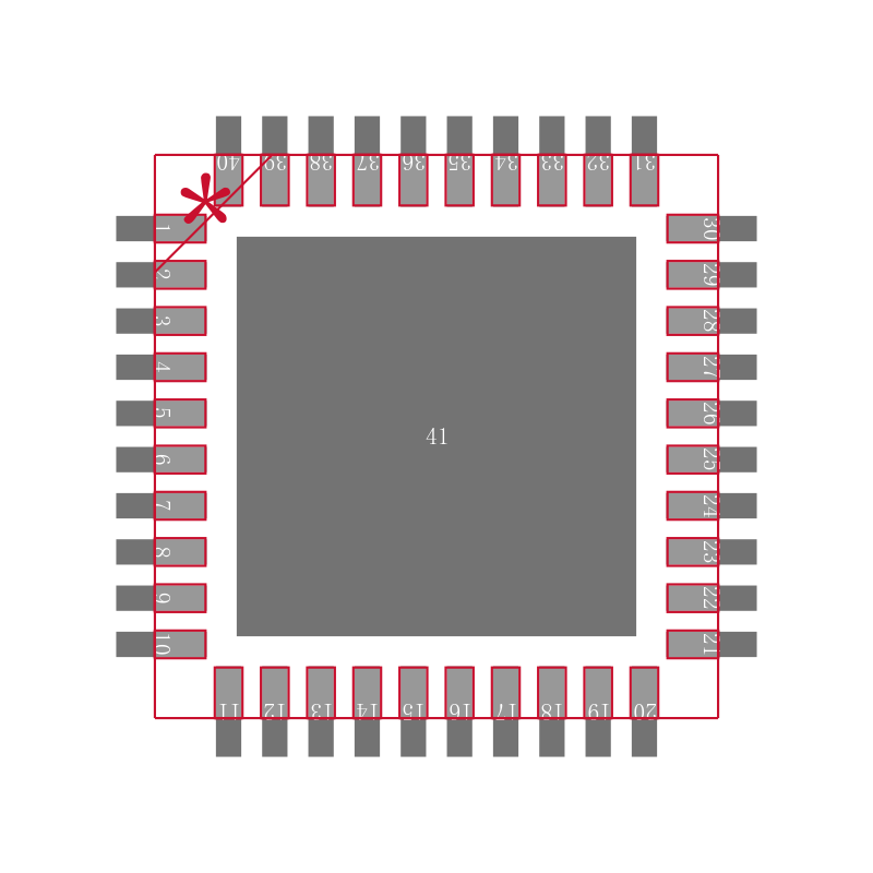
- 40-lead, 6 mm × 6 mm LFCSP package
- .
- −40°C to +125°C junction temperature