


3.3 V和2.5 V LVCMOS高性能时钟缓冲器系列 3.3 V and 2.5 V LVCMOS High-Performance Clock Buffer Family
DESCRIPON
The CDCLVC11xx is a modular, high-performance, low-skew, general purpose clock buffer family from Texas Instruments. The whole family is designed with a modular approach in mind. It is intended to round up TI"s series of LVCMOS clock generators.
There are 7 different fan-out variations, 1:2 to 1:12, available. All of the devices are pin compatible to each other for easy handling. All family members share the same high performing characteristics like low additive jitter, low skew, and wide operating temperature range.
FEATURES
• High-Performance 1:2, 1:3, 1:4, 1:6, 1:8, 1:10, 1:12 LVCMOS Clock Buffer Family
• Very Low Pin-to-Pin Skew < 50 ps
• Very Low Additive Jitter < 100 fs
• Supply Voltage: 3.3 V or 2.5 V
• fmax= 250 MHz for 3.3 V
fmax= 180 MHz for 2.5 V
• Operating Temperature Range: –40°C to 85°C
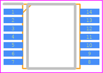
• Available in 8-, 14-, 16-, 20-, 24-Pin TSSOP
Package all pin compatible
APPLICATIONS
• General Purpose Communication, Industrial and Consumer Applications
频率 250 MHz
电源电压DC 2.30V ~ 3.60V
输出接口数 6
电路数 1
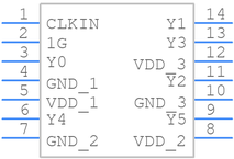
针脚数 14
输出电流驱动 -1.00 mA
工作温度Max 85 ℃
工作温度Min -40 ℃
电源电压 2.3V ~ 3.6V
电源电压Max 3.6 V
电源电压Min 2.3 V
安装方式 Surface Mount
引脚数 14
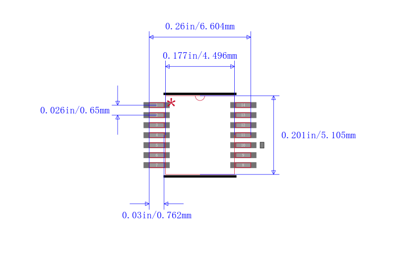
封装 TSSOP-14
高度 1.05 mm
封装 TSSOP-14
工作温度 -40℃ ~ 85℃
产品生命周期 Active
包装方式 Tape & Reel TR
RoHS标准 RoHS Compliant
含铅标准 Lead Free
ECCN代码 EAR99
| 型号/品牌 | 代替类型 | 替代型号对比 |
|---|---|---|
CDCLVC1106PWR TI 德州仪器 | 当前型号 | 当前型号 |
CDCLVC1106PW 德州仪器 | 类似代替 | CDCLVC1106PWR和CDCLVC1106PW的区别 |