


CMOS选通六反相器/缓冲器 CMOS Strobed Hex Inverter/Buffer
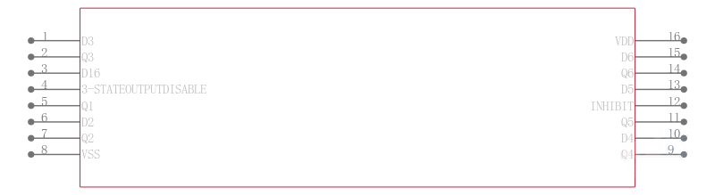
CD4502B consists of six inverter/buffers with 3-state outputs. A logic "1" on the OUTPUT DISABLE input produces a high-impedance state in all six outputs. This feature permits common busing of the outputs, thus simplifying system design. A Logic "1" on the INHIBIT input switches all six outputs to logic "0" if the OUTPUT DISABLE input is a logic "0". This device is capable of driving two standard TTL loads, which is equivalent to six times the JEDEC "B"-series IOL standard.
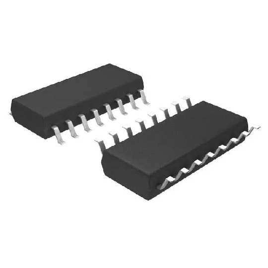
The CD4502B types are supplied in 16-lead hermetic dual-in-line ceramic packages F3A suffix, 16-lead dual-in-line plastic packages E suffix, 16-lead small-outline packages NSR suffix, and 16-lead thin shrink small-outline packages PW and PWR suffixes.
电源电压DC 3.00V ~ 18.0V
输出接口数 6
电路数 6
位数 6
传送延迟时间 380 ns
电压波节 5.00 V, 10.0 V, 15.0 V
耗散功率 500 mW
输出电流驱动 -167 µA
输入数 1
工作温度Max 125 ℃
工作温度Min -55 ℃
耗散功率Max 500 mW
电源电压 3V ~ 18V
安装方式 Surface Mount
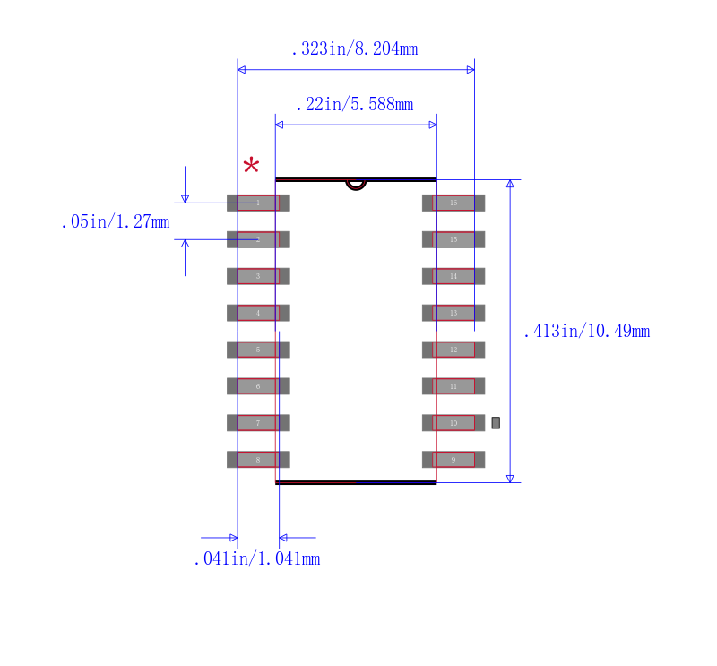
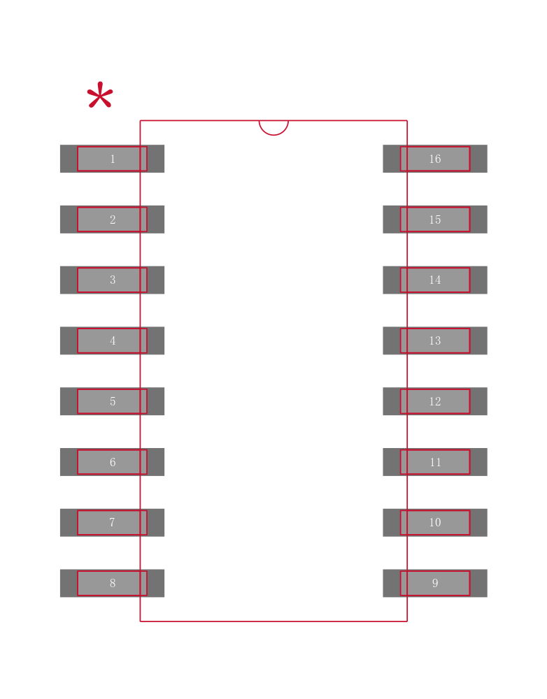
引脚数 16
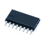
封装 SOP-16
长度 10.3 mm
宽度 5.3 mm
高度 1.95 mm
封装 SOP-16
工作温度 -55℃ ~ 125℃
产品生命周期 Active
包装方式 Tape & Reel TR
RoHS标准 RoHS Compliant
含铅标准 Lead Free