9兆位( 256K ×36 / 512K ×18 )流水线式SRAM 9-Mbit 256K x 36/512K x 18 Pipelined SRAM
Functional Description
The CY7C1360B/CY7C1362B SRAM integrates 262,144 x 36 and 524,288 x 18 SRAM cells with advanced synchronous peripheral circuitry and a two-bit counter for internal burst operation. All synchronous inputs are gated by registers controlled by a positive-edge-triggered Clock Input CLK. The synchronous inputs include all addresses, all data inputs, address-pipelining Chip Enable CE1, depth-expansion Chip Enables CE2and CE3 [2], Burst Control inputs ADSC, ADSP, and ADV, Write Enables BWX, and BWE, and Global Write GW. Asynchronous inputs include the Output Enable OE and the ZZ pin.
Features
• Supports bus operation up to 225 MHz
• Available speed grades are 225, 200 and 166 MHz
• Registered inputs and outputs for pipelined operation
• 3.3V core power supply
• 2.5V/3.3V I/O operation
• Fast clock-to-output times
— 2.8 ns for 225-MHz device
— 3.0 ns for 200-MHz device
— 3.5 ns for 166-MHz device
• Provide high-performance 3-1-1-1 access rate
• User-selectable burst counter supporting Intel Pentium® interleaved or linear burst sequences
• Separate processor and controller address strobes
• Synchronous self-timed writes
• Asynchronous output enable
• Single Cycle Chip Deselect
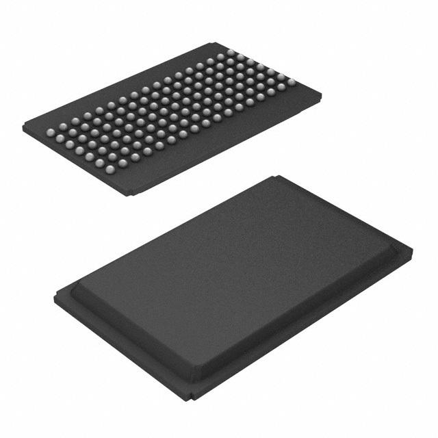
• Offered in JEDEC-standard 100-pin TQFP, 119-ball BGA and 165-Ball fBGA packages
• TQFP Available with 3-Chip Enable and 2-Chip Enable
• IEEE 1149.1 JTAG-Compatible Boundary Scan
• “ZZ” Sleep Mode Option