

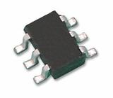
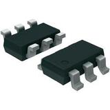

FAIRCHILD SEMICONDUCTOR FDC6310P 双路场效应管, MOSFET, 双P沟道, -2.2 A, -20 V, 0.1 ohm, -4.5 V, -1 V
The is a dual P-channel MOSFET produced using advanced PowerTrench® process. It has been especially tailored to minimize ON-state resistance and yet maintain low gate charge for superior switching performance. This device has been designed to offer exceptional power dissipation in a very small footprint for applications where the bigger more expensive packages are impractical. It is suitable for use with load switch and battery protected applications.
- .
- Low gate charge
- .
- Fast switching speed
- .
- High performance Trench technology for extremely low RDS ON
- .
- Small footprint
- .
- Low profile
额定电压DC -20.0 V
额定电流 -2.20 A
通道数 2
针脚数 6
漏源极电阻 0.1 Ω
极性 Dual P-Channel, P-Channel
耗散功率 960 mW
输入电容 337 pF
栅电荷 3.70 nC
漏源极电压Vds 20 V
漏源击穿电压 20 V
栅源击穿电压 ±12.0 V
连续漏极电流Ids 2.20 A
上升时间 12 ns
输入电容Ciss 337pF @10VVds
额定功率Max 700 mW
下降时间 5 ns
工作温度Max 150 ℃
工作温度Min -55 ℃
耗散功率Max 0.96 W
安装方式 Surface Mount
引脚数 6
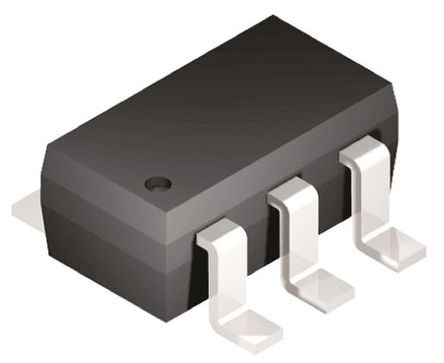
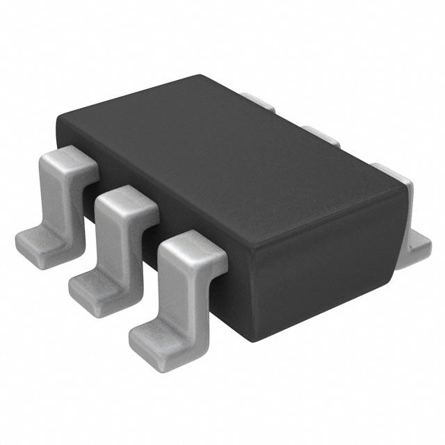
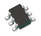
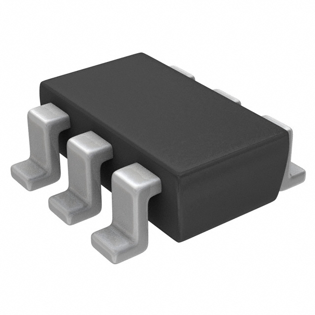
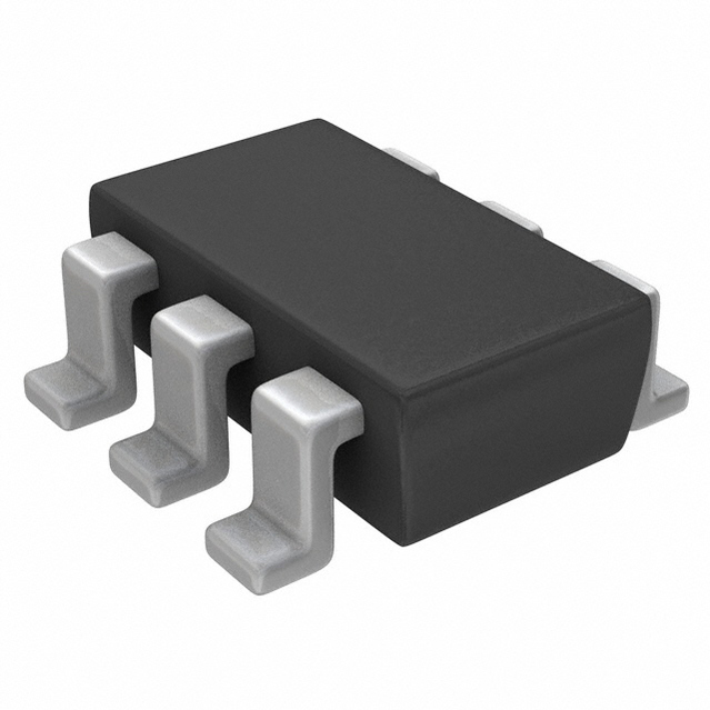
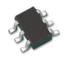
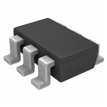
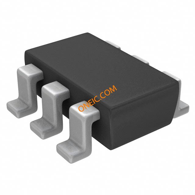
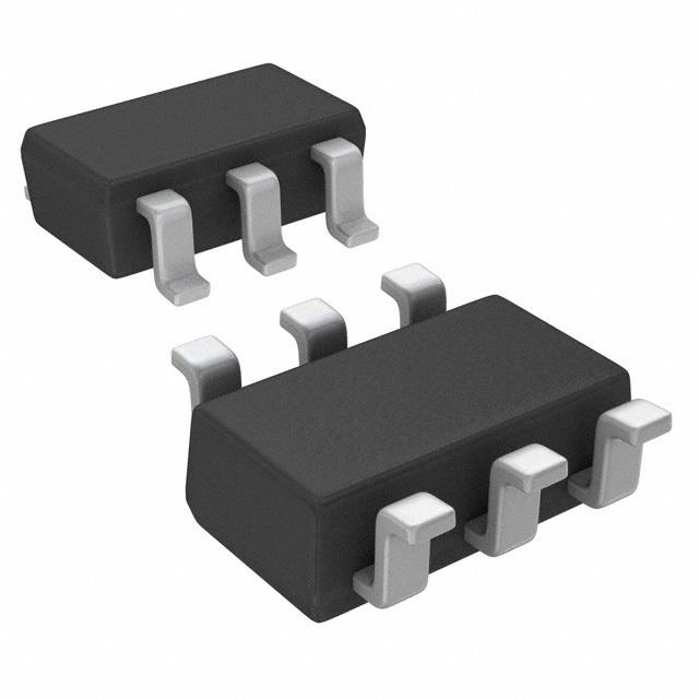
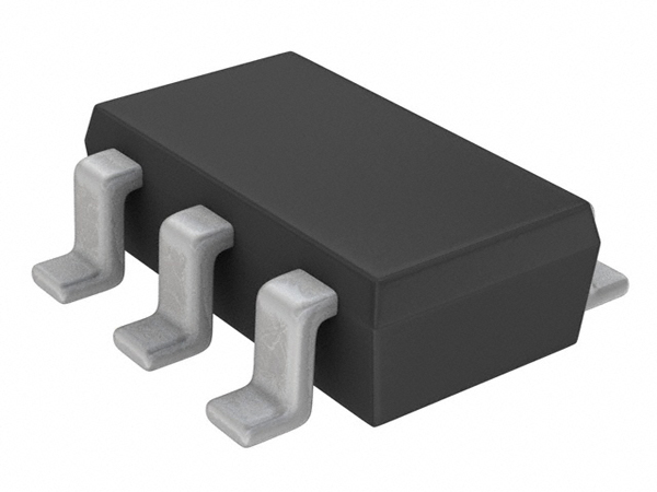
封装 TSOT-23-6
长度 3 mm
宽度 1.7 mm
高度 1 mm
封装 TSOT-23-6
工作温度 -55℃ ~ 150℃ TJ
产品生命周期 Unknown
包装方式 Tape & Reel TR
RoHS标准 RoHS Compliant
含铅标准 Lead Free
REACH SVHC标准 No SVHC
REACH SVHC版本 2015/06/15
ECCN代码 EAR99