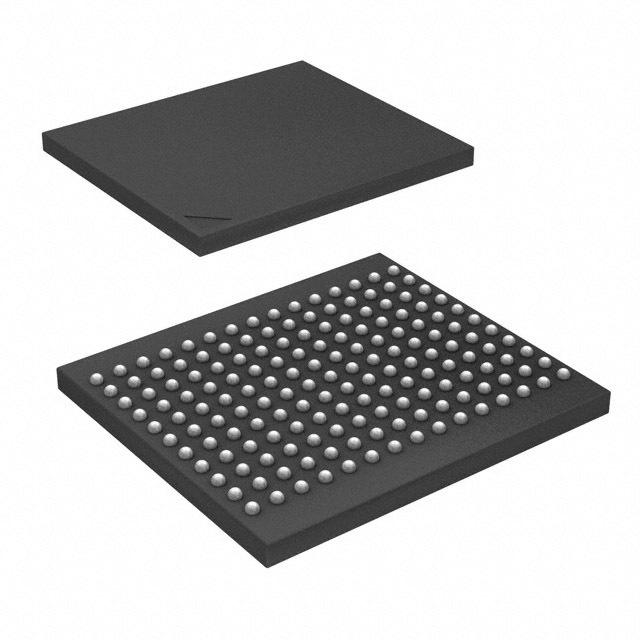
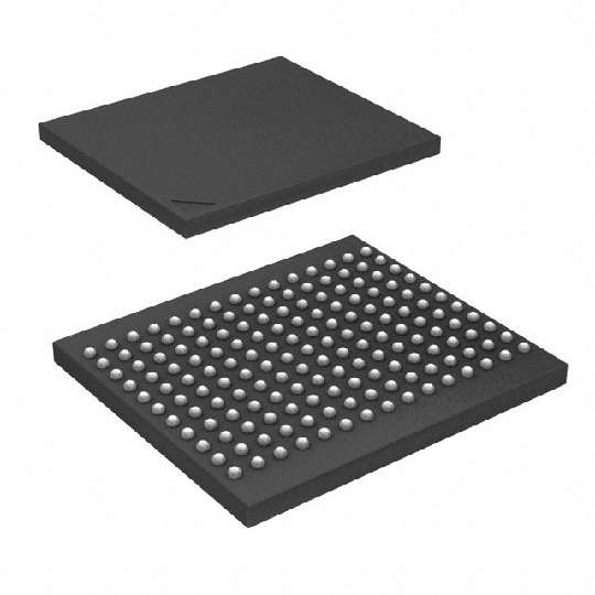
SRAM Chip Sync 3.3V 18M-bit 1M x 18 3ns 165Pin TFBGA
* 100 percent bus utilization * No wait cycles between Read and Write * Internal self-timed write cycle * Individual Byte Write Control * Single R/W Read/Write control pin * Clock controlled, registered address, data and control * Interleaved or linear burst sequence control using MODE input * Three chip enables for simple depth expansion and address pipelining * Power Down mode * Common data inputs and data outputs * /CKE pin to enable clock and suspend operation * JEDEC 100-pin QFP, 165-ball BGA and 119- ball BGA packages * Power supply * Vdd 3.3V ± 5%, Vddq 3.3V/2.5V ± 5% * JTAG Boundary Scan for BGA packages * Commercial, Industrial and Automotive x36 temperature support * Lead-free available.