


INFINEON IPB011N04NGATMA1 晶体管, MOSFET, N沟道, 180 A, 40 V, 0.0009 ohm, 10 V, 4 V
I OptiMOS™3 功率 MOSFET,高达 40V
OptiMOS™产品提供高效能封装,以解决最具挑战性的应用,在有限空间内提供完全的灵活性。 这些 Infineon 产品经的设计符合并超过计算机应用中更严格的下一代电压调节标准的能效和功率密度要求。
快速切换 MOSFET,用于 SMPS
优化技术,用于直流/直流转换器
符合目标应用的 JEDEC1 规格
N 通道,逻辑电平
极佳的栅极电荷 x R DSon 产品 FOM
极低导通电阻 R DSon
无铅电镀
欧时:
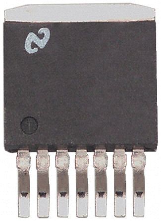
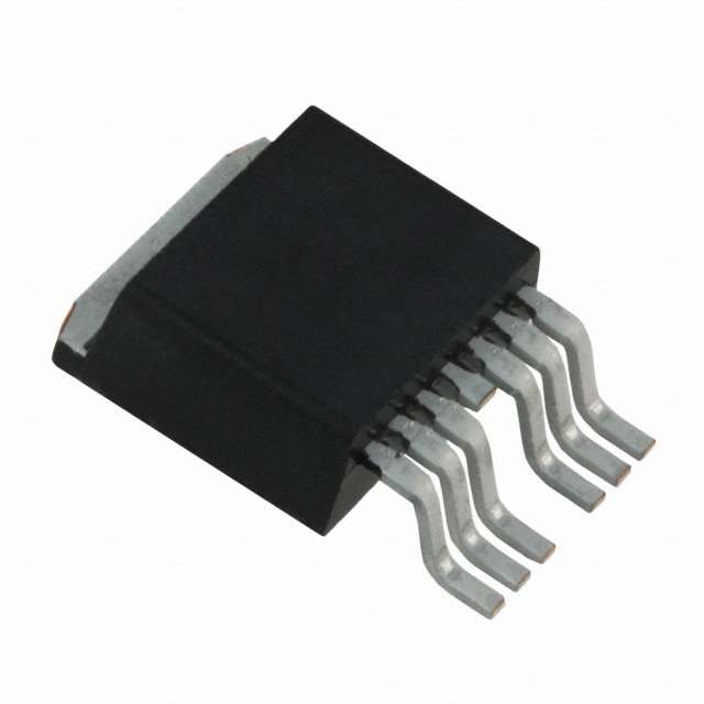
Infineon OptiMOS 3 系列 Si N沟道 MOSFET IPB011N04NGATMA1, 180 A, Vds=40 V, 7引脚 D2PAK TO-263封装
得捷:
MOSFET N-CH 40V 180A TO263-7
立创商城:
N沟道 40V 180A
艾睿:
Amplify electronic signals and switch between them with the help of Infineon Technologies&s; IPB011N04NGATMA1 power MOSFET. Its maximum power dissipation is 250000 mW. Tape and reel packaging will encase this product during shipment, in order to ensure safe delivery and enable quick mounting of components. This N channel MOSFET transistor operates in enhancement mode. This MOSFET transistor has a minimum operating temperature of -55 °C and a maximum of 175 °C. This device is made with optimos technology.
TME:
Transistor: N-MOSFET; unipolar; 40V; 180A; 250W; PG-TO263-7
Verical:
Trans MOSFET N-CH 40V 180A 7-Pin6+Tab D2PAK T/R
Newark:
# INFINEON IPB011N04NGATMA1 MOSFET Transistor, N Channel, 180 A, 40 V, 0.0009 ohm, 10 V, 4 V
额定功率 250 W
针脚数 7
极性 N-Channel
耗散功率 250 W
阈值电压 4 V
漏源极电压Vds 40 V
连续漏极电流Ids 180A
上升时间 10 ns
输入电容Ciss 16000pF @20VVds
下降时间 13 ns
工作温度Max 175 ℃
工作温度Min -55 ℃
耗散功率Max 250W Tc
安装方式 Surface Mount
引脚数 7
封装 TO-263-7
长度 10.31 mm
宽度 9.45 mm
高度 4.57 mm
封装 TO-263-7
工作温度 -55℃ ~ 175℃ TJ
产品生命周期 Active
包装方式 Tape & Reel TR
制造应用 工业, Isolated DC-DC converters, Industrial, Synchronous rectification, 电源管理, Or-ing switches, Power Management, Motor Drive & Control, 电机驱动与控制
RoHS标准
含铅标准 Lead Free
REACH SVHC标准 No SVHC
REACH SVHC版本 2015/12/17