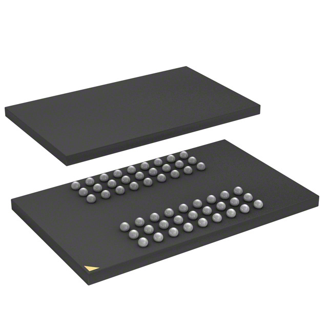
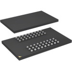
DRAM Chip Mobile SDRAM 256Mbit 16Mx16 2.5V 54Pin TFBGA
SDRAM - 移动 存储器 IC 256Mb(16M x 16) 并联 143 MHz 5.4 ns 54-TFBGA(8x13)
得捷:
IC DRAM 256MBIT PAR 54TFBGA
艾睿:
DRAM Chip Mobile SDRAM 256Mbit 16Mx16 2.5V 54-Pin TFBGA
安富利:
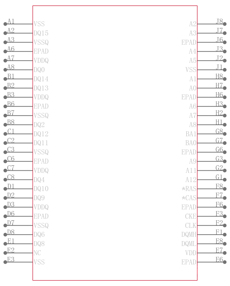
ISSI"s 256Mb Mobile Synchronous DRAM achieves highspeed data transfer using pipeline architecture. All input and output signals the rising edge of the clock input. Both write and read accesses to the SDRAM are burst oriented. The 256Mb Mobile Synchronous DRAM is designed to minimize current consumption making it ideal for low-power applications. Both TSOP and BGA packages are offered, including industrial grade products.ISSI’s 256Mb SDRAM is a high speed CMOS, dynamic random-access memory designed to operate in 3.3V – 2.5V VDD and 3.3V – 2.5V VDDQ memory systems containing 268,435,456 bits. Internally configured as a quad-bank DRAM with a synchronous interface. The 256Mb SDRAM includes an AUTO REFRESH MODE, and a power-saving, power-down mode. All signals are registered on the positive edge of the clock signal, CLK. All inputs and outputs are LVTTL VDD = 3.3V or LVCMOS VDD = 2.5V compatible. The 256Mb SDRAM has the ability to synchronously burst data at a high data rate with automatic column-address generation, the ability to interleave between internal banks to hide precharge time and the capability to randomly change column addresses on each clock cycle during burst access.A self-timed row precharge initiated at the end of the burst sequence is available with the AUTO PRECHARGE function enabled. Precharge one bank while accessing one of the other three banks will hide the precharge cycles and provide seamless, high-speed, random-access operation. SDRAM read and write accesses are burst oriented starting at a selected location and continuing for a programmed number of locations in a programmed sequence. The registration of an Active command begins accesses, followed by a Read or Write command. The ACTIVE command in conjunction with address bits registered are used to select the bank and row to be accessed BA0, BA1 select the bank; A0-A12 x8 and x16 and A0-A11 x32 select the row. The READ or WRITE commands in conjunction with address bits registered are used to select the starting column location for the burst access. Programmable READ or WRITE burst lengths consist of 1, 2, 4 and 8 locations, or full page, with a burst terminate option.
Chip1Stop:
DRAM Chip Mobile SDRAM 256M-Bit 16Mx16 2.5V 54-Pin TFBGA
Verical:
DRAM Chip Mobile SDRAM 256Mbit 16Mx16 2.5V 54-Pin TFBGA
Win Source:
IC SDRAM 256M 143MHZ 54BGA
| 型号/品牌 | 代替类型 | 替代型号对比 |
|---|---|---|
IS42RM16160D-7BLI Integrated Silicon SolutionISSI | 当前型号 | 当前型号 |
IS42RM16160D-7BL Integrated Silicon SolutionISSI | 完全替代 | IS42RM16160D-7BLI和IS42RM16160D-7BL的区别 |
IS42RM16160K-6BLI Integrated Silicon SolutionISSI | 功能相似 | IS42RM16160D-7BLI和IS42RM16160K-6BLI的区别 |
IS42RM16160D-75BLI Integrated Silicon SolutionISSI | 功能相似 | IS42RM16160D-7BLI和IS42RM16160D-75BLI的区别 |