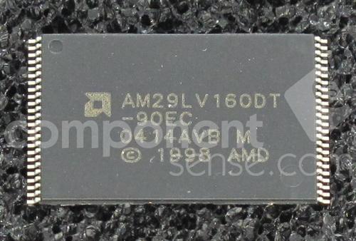
16-Mbit2M x 8bit/1M x 16bit,并行接口,工作电压:2.7V to 3.6V
GENERAL DESCRIPTION
The Am29LV160D is a 16 Mbit, 3.0 Volt-only Flash memory organized as 2,097,152 bytes or 1,048,576 words. The device is offered in 48-ball FBGA, 44-pin SO, and 48-pin TSOP packages. The word-wide data x16 appears on DQ15–DQ0; the byte-wide x8 data appears on DQ7–DQ0. This device is designed to be programmed in-system with the standard system 3.0 volt VCC supply. A 12.0 V VPP or 5.0 VCC are not required for write or erase operations. The device can also be programmed in standard EPROM programmers.
DISTINCTIVE CHARACTERISTICS
■ Single power supply operation
— Full voltage range: 2.7 to 3.6 volt read and write operations for battery-powered applications
— Regulated voltage range: 3.0 to 3.6 volt read and write operations and for compatibility with high performance 3.3 volt microprocessors
■ Manufactured on 0.23 µm process technology
— Fully compatible with 0.32 µm Am29LV160B device
■ High performance
— Access times as fast as 70 ns
■ Ultra low power consumption typical values at 5 MHz
— 200 nA Automatic Sleep mode current
— 200 nA standby mode current
— 9 mA read current
— 20 mA program/erase current
■ Flexible sector architecture
— One 16 Kbyte, two 8 Kbyte, one 32 Kbyte, and thirty-one 64 Kbyte sectors byte mode
— One 8 Kword, two 4 Kword, one 16 Kword, and thirty-one 32 Kword sectors word mode
— Supports full chip erase
— Sector Protection features:
— A hardware method of locking a sector to prevent any program or erase operations within that sector
— Sectors can be locked in-system or via programming equipment Temporary Sector Unprotect feature allows code changes in previously locked sectors
■ Unlock Bypass Program Command
— Reduces overall programming time when issuing multiple program command sequences
■ Top or bottom boot block configurations available
■ Embedded Algorithms
— Embedded Erase algorithm automatically preprograms and erases the entire chip or any combination of designated sectors
— Embedded Program algorithm automatically writes and verifies data at specified addresses
■ Minimum 1,000,000 write cycle guarantee per sector
■ 20-year data retention at 125°C
— Reliable operation for the life of the system
■ Package option
— 48-ball FBGA
— 48-pin TSOP
— 44-pin SO
■ CFI Common Flash Interface compliant
— Provides device-specific information to the system, allowing host software to easily reconfigure for different Flash devices
■ Compatibility with JEDEC standards
— Pinout and software compatible with single power supply Flash
— Superior inadvertent write protection
■ Data# Polling and toggle bits
— Provides a software method of detecting program or erase operation completion
■ Ready/Busy# pin RY/BY#
— Provides a hardware method of detecting program or erase cycle completion not available on 44-pin SO
■ Erase Suspend/Erase Resume
— Suspends an erase operation to read data from, or program data to, a sector that is not being erased, then resumes the erase operation
■ Hardware reset pin RESET#
— Hardware method to reset the device to reading array data