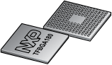


LPC3141FET180 - ARM926EJ-S,带192 kB SRAM、高速USB OTG、SD/MMC以及NAND闪存控制器
Overview
The LPC3141 combine a 270 MHz ARM926EJ-S CPU core, High-speed USB 2.0 OTG, 192 kB SRAM, NAND flash controller, flexible external bus interface, four channel 10-bit A/D, and a myriad of serial and parallel interfaces in a single chip targeted at consumer, industrial, medical, and communication markets. To optimize system power consumption, the LPC3141 have multiple power domains and a very flexible Clock
MoreLess
## Features
* 270 MHz, 32-bit ARM926EJ-S
* 16 kB D-cache and 16 kB I-cache
* Memory Management Unit MMU
* 192 kB embedded SRAM
* 8/16-bit Multi-Port Memory Controller MPMC: SDRAM and SRAM
* High-speed USB 2.0 OTG, Host, Device with on-chip PHY
* Two I2S interfaces
* Integrated master/slave SPI
* Two master/slave I2C-bus interfaces
* Fast UART
* Memory Card Interface MCI: MMC/SD/SDIO/CE-ATA
* Four-channel 10-bit ADC
* Integrated 4/8/16-bit 6800/8080 compatible LCD interface
* Dynamic clock gating and scaling
* Multiple power domains
* Selectable boot-up: SPI flash, NAND flash, SD/MMC cards, UART, or USB
* DMA controller
* Four 32-bit timers
* Watchdog timer
* PWM module
* Master/slave PCM interface
* Random Number Generator RNG
* General Purpose I/O pins GPIO
* Flexible and versatile interrupt structure
* JTAG interface with boundary scan and ARM debug access
* Core voltage: 1.2 V
* I/O voltages: 1.8 V, 3.3 V
## Target Applications
* Industrial control
* Communications
* Medical systems
* Intelligent washing machine
* LCD display - discretes focus
* Protocol converter
## Features
电源电压DC 1.10V min
时钟频率 270 MHz
RAM大小 192K x 8
模数转换数ADC 1
工作温度Max 85 ℃
工作温度Min 40 ℃
电源电压 3.6 V
电源电压Max 1.3 V
电源电压Min 1.1 V
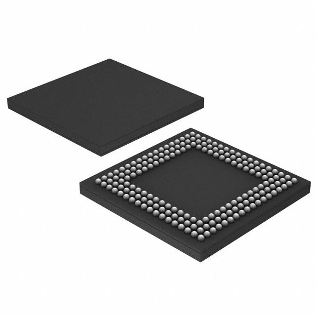
安装方式 Surface Mount
引脚数 180
封装 TFBGA-180
封装 TFBGA-180
工作温度 -40℃ ~ 85℃
产品生命周期 Active
包装方式 Tray
RoHS标准 RoHS Compliant
含铅标准 Lead Free
REACH SVHC标准 No SVHC
REACH SVHC版本 2015/12/17
| 型号/品牌 | 代替类型 | 替代型号对比 |
|---|---|---|
LPC3141FET180,551 NXP 恩智浦 | 当前型号 | 当前型号 |
LPC3143FET180,551 恩智浦 | 类似代替 | LPC3141FET180,551和LPC3143FET180,551的区别 |