

晶体管 双极预偏置/数字, NPN和PNP执行, 50 V, 100 mA, 2.2 kohm, 47 kohm, 0.047 电阻比率
Are you designing a digital processing circuit and are looking to apply the characteristics of traditional BJT"s within? Look no further than the npn and PNP digital transistor from . This product"s maximum continuous DC collector current is 100 mA, while its minimum DC current gain is 80@5mA@10 V. It has a maximum collector emitter saturation voltage of 0.25@0.3mA@10mA V. It has a maximum collector emitter voltage of 50 V. Its maximum power dissipation is 385 mW. Tape and reel packaging will encase the product during shipment, ensuring safe delivery and enabling quick mounting of components. It is made in a dual configuration. This transistor has a minimum operating temperature of -55 °C and a maximum of 150 °C.
额定电压DC 50.0 V
额定电流 100 mA
极性 NPN+PNP
耗散功率 0.385 W
击穿电压集电极-发射极 50 V
集电极最大允许电流 100mA
最小电流放大倍数hFE 80 @5mA, 10V
额定功率Max 250 mW
工作温度Max 150 ℃
工作温度Min -55 ℃
耗散功率Max 385 mW
安装方式 Surface Mount
引脚数 6
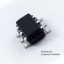
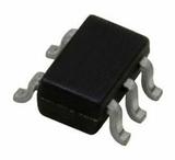
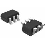
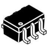
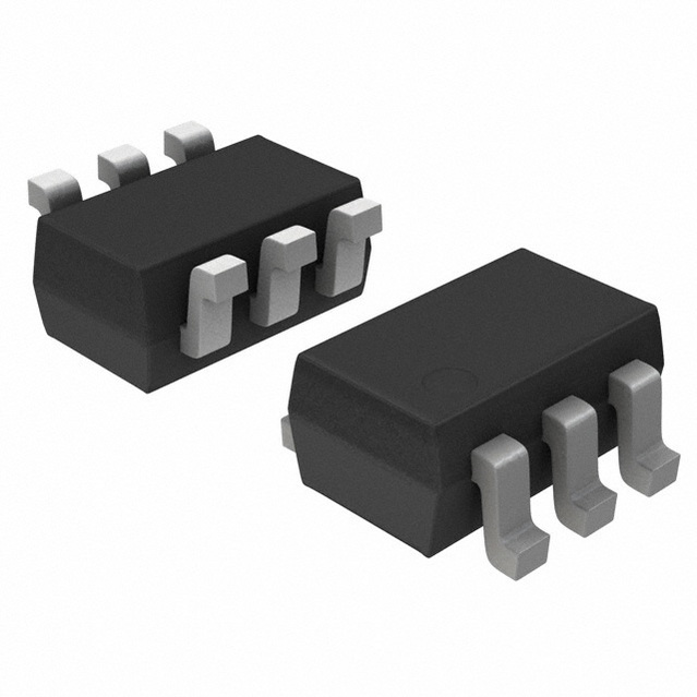
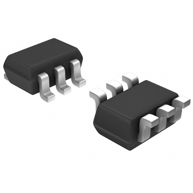
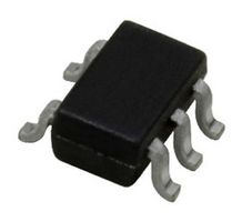
封装 SC-70-6
封装 SC-70-6
工作温度 -55℃ ~ 150℃
产品生命周期 Active
包装方式 Tape & Reel TR
RoHS标准 RoHS Compliant
含铅标准 Lead Free
REACH SVHC版本 2015/12/17
ECCN代码 EAR99
| 型号/品牌 | 代替类型 | 替代型号对比 |
|---|---|---|
MUN5335DW1T2G ON Semiconductor 安森美 | 当前型号 | 当前型号 |
MUN5335DW1T2 安森美 | 完全替代 | MUN5335DW1T2G和MUN5335DW1T2的区别 |
MUN5335DW1T1G 安森美 | 类似代替 | MUN5335DW1T2G和MUN5335DW1T1G的区别 |
DCX123JU-7-F 美台 | 功能相似 | MUN5335DW1T2G和DCX123JU-7-F的区别 |