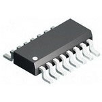

8级移位/存储寄存器具有三态输出 8-Stage Shift/Store Register with Three-State Outputs
The MC14094B combines an 8–stage shift register with a data latch for each stage and a three–state output from each latch. Data is shifted on the positive clock transition and is shifted from the seventh stage to two serial outputs. The QSoutput data is for use in high–speed cascaded systems. The Q′Soutput data is shifted on the following negative clock transition for use in low–speed cascaded systems. Data from each stage of the shift register is latched on the negative
transition of the strobe input. Data propagates through the latch while strobe is high. Outputs of the eight data latches are controlled by three–state buffers which are placed in the high impedance state by a logic Low on Output Enable.
•Three–State Outputs
•Capable of Driving Two Low–Power TTL Loads or One Low–Power Schottky TTL Load Over the Rated Temperature Range
•Input Diode Protection
•Data Latch
•Dual Outputs for Data Out on Both Positive and
Negative Clock Transitions
•Useful for Serial–to–Parallel Data Conversion
•Pin–for–Pin Compatible with CD4094B
| 型号/品牌 | 代替类型 | 替代型号对比 |
|---|---|---|
MC14094BD ON Semiconductor 安森美 | 当前型号 | 当前型号 |
MC14094BDR2G 安森美 | 完全替代 | MC14094BD和MC14094BDR2G的区别 |
MC14094BDR2 安森美 | 完全替代 | MC14094BD和MC14094BDR2的区别 |
MC14094BDG 安森美 | 类似代替 | MC14094BD和MC14094BDG的区别 |