
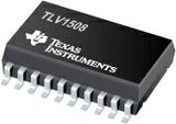
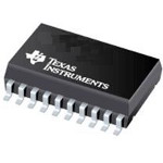


2.7 V至5.5 V , 10位, 200 KSPS , 4/8通道,低功耗,串行模拟数字转换器具有自动关机 2.7 V TO 5.5 V, 10-BIT, 200 KSPS, 4/8 CHANNEL, LOW POWER, SERIAL ANALOG-TO-DIGITAL CONVERTERS WITH AUTO POWER DOWN
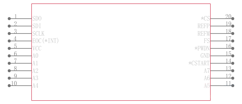
The TLV1508 and TLV1504 are a family of high performance, 10-bit low power, 3.86 µs, CMOS analog-to-digital converters ADC which operate from a single 2.7-V to 5.5-V power supply. These devices have three digital inputs and a 3-state output [chip select CS\, serial input-output clock SCLK, serial data input SDI, and serial data output SDO] that provide a direct 4-wire interface to the serial port of most popular host microprocessors SPI interface. When interfaced with a TMS320 DSP, a frame sync FS signal is used to indicate the start of a serial data frame.
In addition to a high-speed A/D converter and versatile control capability, these devices have an on-chip analog multiplexer that can select any analog inputs or one of three internal self-test voltages. The sample-and-hold function is automatically started after the fourth SCLK edge normal sampling or can be controlled by a special pin, CSTART\, to extend the sampling period extended sampling. The normal sampling period can also be programmed as short 12 SCLKs or as long 24 SCLKs to accommodate faster SCLK operation popular among high-performance signal processors. The TLV1508 and TLV1504 are designed to operate with very low power consumption. The power-saving feature is further enhanced with software/hardware/autopower-down modes and programmable conversion speeds. The conversion clock OSC and reference are built-in. The converter can use the external SCLK as the source of the conversion clock to achieve higher up to 2.8 µs when a 20 MHz SCLK is used conversion speed. Two different internal reference voltages are available. An optional external reference can also be used to achieve maximum flexibility.
The TLV1504I and the TLV1508I are characterized for operation from 40°C to 85°C.
数字逻辑电平 SAR
电源电压DC 2.70V min
输出电压 2.40 V
供电电流 2.10 mA
电路数 1
位数 10
耗散功率 1294 W
采样率 200 ksps
功耗 3.30 mW
模数转换数ADC 1
输入数 4
工作温度Max 85 ℃
工作温度Min -40 ℃
耗散功率Max 1294 mW
输入通道数 8
电源电压Max 5.5 V
电源电压Min 2.7 V
输入电压 3.3 V
安装方式 Surface Mount
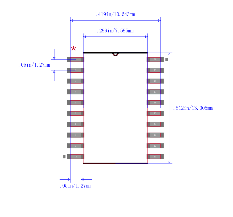
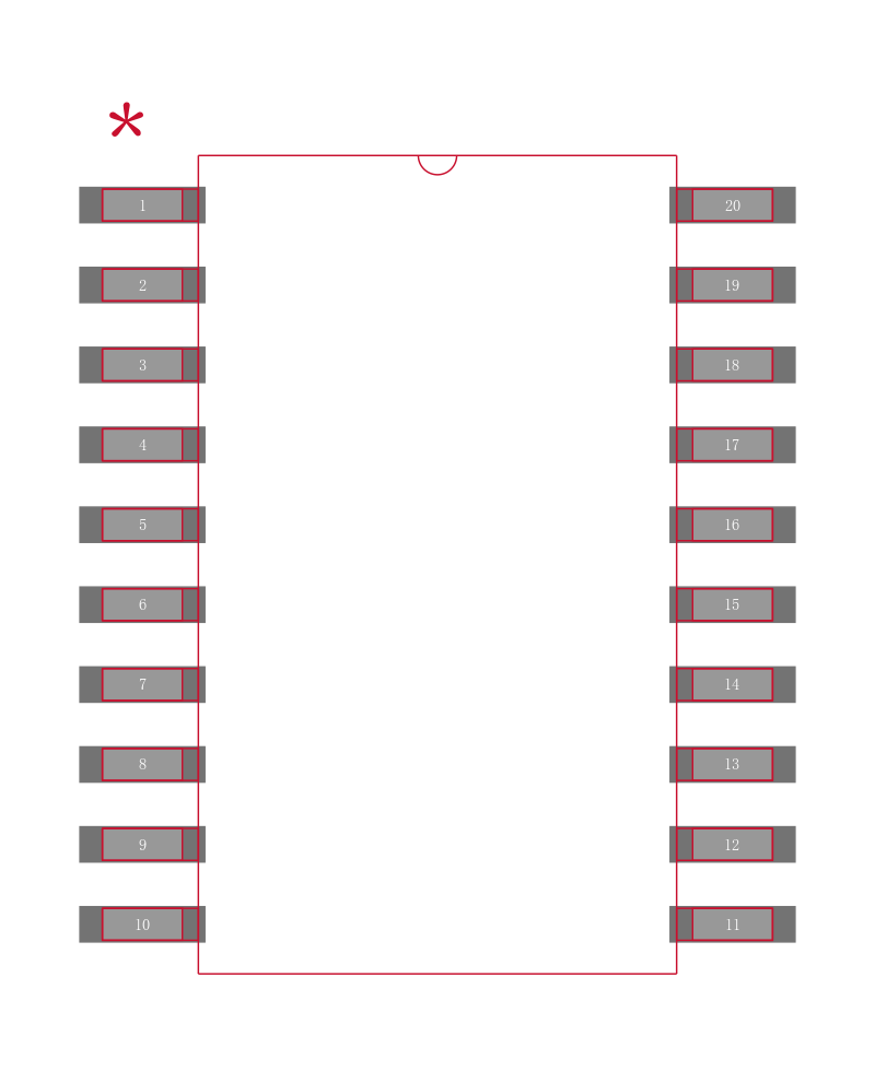
引脚数 20
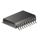
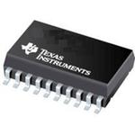
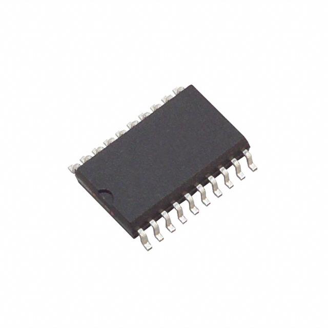
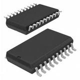
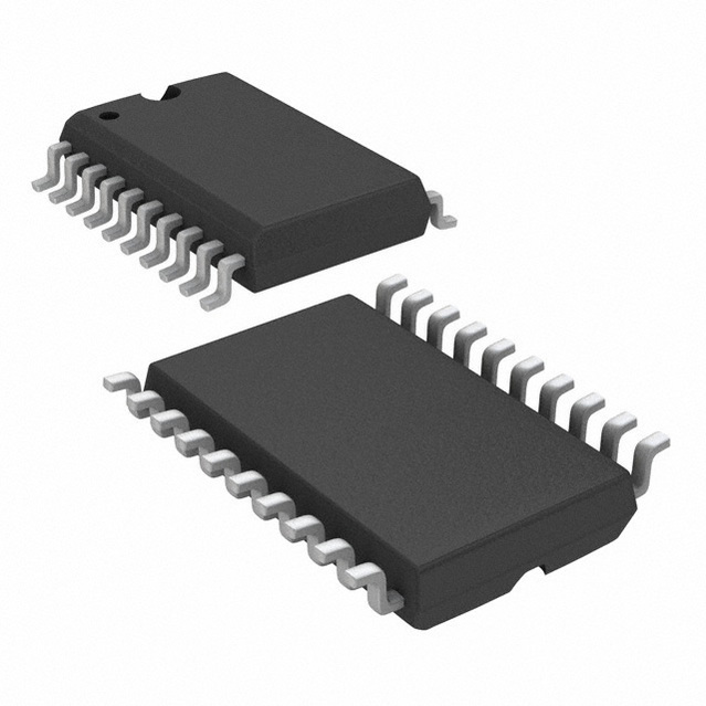
封装 SOIC-20
封装 SOIC-20
工作温度 -40℃ ~ 85℃
产品生命周期 Active
包装方式 Tube
RoHS标准 RoHS Compliant
含铅标准 Lead Free
REACH SVHC版本 2015/06/15
ECCN代码 EAR99
| 型号/品牌 | 代替类型 | 替代型号对比 |
|---|---|---|
TLV1508IDW TI 德州仪器 | 当前型号 | 当前型号 |
TLV2548IDW 德州仪器 | 完全替代 | TLV1508IDW和TLV2548IDW的区别 |
TLV2548CDW 德州仪器 | 完全替代 | TLV1508IDW和TLV2548CDW的区别 |
TLV1508IDWG4 德州仪器 | 完全替代 | TLV1508IDW和TLV1508IDWG4的区别 |