


J-K 下降沿触发 双稳态触发器 带 5 V 容差输入
General Description
The LCX112 is a dual J-K flip-flop. Each flip-flop has inde pendent J, K, PRESET, CLEAR, and CLOCK inputs with Q, Q outputs. These devices are edge sensitive and change state on the negative going transition of the clock pulse. Clear and preset are independent of the clock and accomplished by a low logic level on the corresponding input. LCX devices are designed for low voltage 3.3V or 2.5 operation with the added capability of interfacing to a 5V signal environment.
The 74LCX112 is fabricated with advanced CMOS technology to achieve high speed operation while maintaining CMOS low power dissipation.
Features
■ 5V tolerant inputs
■ 2.3V–3.6V VCC specifications provided
■ 7.5 ns tPD max VCC = 3.3V, 10 µA ICC max
■ Power down high impedance inputs and outputs
■ ±24 mA output drive VCC = 3.0V
■ Implements patented noise/EMI reduction circuitry
■ Latch-up performance exceeds 500 mA
■ ESD performance:
Human body model > 2000V
Machine model > 2000V
频率 150 MHz
电源电压DC 3.30 V
电路数 2
时钟频率 150 MHz
位数 2
极性 Non-Inverting, Inverting
输入电容 7 pF
工作温度Max 85 ℃
工作温度Min -40 ℃
电源电压 2V ~ 3.6V
电源电压Max 3.6 V
电源电压Min 2 V
安装方式 Surface Mount
引脚数 16
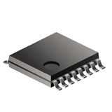
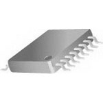
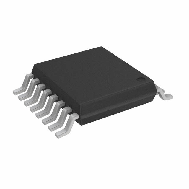
封装 TSSOP-16
高度 0.9 mm
封装 TSSOP-16
工作温度 -40℃ ~ 85℃ TA
产品生命周期 Active
包装方式 Tape & Reel TR
RoHS标准 RoHS Compliant
含铅标准 Lead Free
ECCN代码 EAR99