低相位噪声,快速建立, 6 GHz的 Low Phase Noise, Fast Settling, 6 GHz
Product Details
The ADF4196 frequency synthesizer can be used to implement local oscillators LO in the upconversion and downconversion sections of wireless receivers and transmitters. Its architecture is specifically designed to meet the GSM/EDGE lock time requirements for base stations, and the fast settling feature makes the ADF4196 suitable for pulse Doppler radar applications.
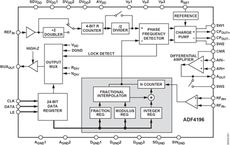
The ADF4196 consists of a low noise, digital phase frequency detector PFD and a precision differential charge pump. A differential amplifier converts the differential charge pump output to a single-ended voltage for the external voltage controlled oscillator VCO. The sigma-delta Σ-Δ based fractional interpolator, working with the N divider, allows programmable modulus fractional-N division. Additionally, the 4-bit reference R counter and on-chip frequency doubler allow selectable reference signal REFIN frequencies at the PFD input.
A complete phase-locked loop PLL can be implemented if the synthesizer is used with an external loop filter and a VCO. The switching architecture ensures that the PLL settles within the GSM time slot guard period, removing the need for a second PLL and associated isolation switches. This decreases the cost, complexity, PCB area, shielding, and characterization found on previous ping-pong GSM PLL architectures.
**Applications**
- .
- GSM/EDGE base stations
- .
- PHS base stations
- .
- Pulsed Doppler radar
- .
- Instrumentation and test equipment
- .
- Beam-forming/phased array systems
### Features and Benefits
- .
- Fast settling, fractional-N
PLL architecture
- .
- Single PLL replaces ping-pong synthesizers
- .
- Frequency hop across GSM band in 5 μs with phase settled within 20 μs
- .
- 1 degree rms phase error at 4 GHz RF output
- .
- Digitally programmable output phase
- .
- RF input range up to 6 GHz
- .
- 3-wire serial interface
- .
- On-chip, low noise differential amplifier
- .
- Phase noise figure of merit: –216 dBc/Hz
频率 6 GHz
输出接口数 3
供电电流 68 mA
电路数 1
工作温度Max 85 ℃
工作温度Min -40 ℃
电源电压 2.7V ~ 3.3V
电源电压Max 3.3 V
电源电压Min 2.7 V
安装方式 Surface Mount
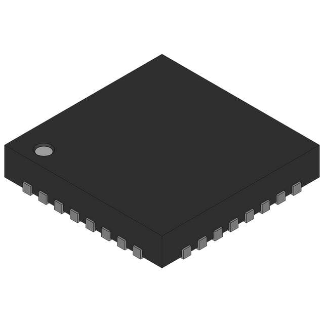
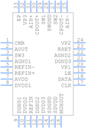
引脚数 32
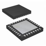
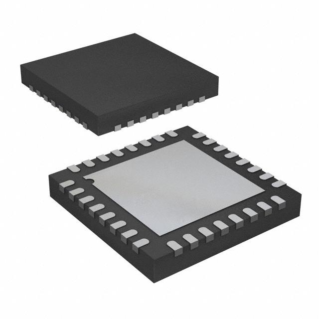
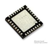
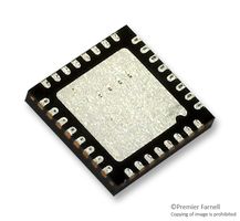
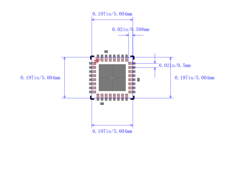
封装 LFCSP EP-32
封装 LFCSP EP-32
工作温度 -40℃ ~ 85℃
产品生命周期 Active
包装方式 Tray
制造应用 Aerospace and Defense, Milcom, Missiles and Precision Munitions
RoHS标准 RoHS Compliant
含铅标准 Lead Free
REACH SVHC标准 No SVHC
REACH SVHC版本 2013/06/20
ECCN代码 5A991.b
| 型号/品牌 | 代替类型 | 替代型号对比 |
|---|---|---|
ADF4196BCPZ ADI 亚德诺 | 当前型号 | 当前型号 |
ADF4196BCPZ-RL7 亚德诺 | 功能相似 | ADF4196BCPZ和ADF4196BCPZ-RL7的区别 |