具有三态输出的 4 位 D 类寄存器
The "173 and "LS173A 4-bit registers include D-type flip-flops featuring totem-pole 3-state outputs capable of driving highly capacitive
or relatively low-impedance loads. The high-impedance third state and increased high-logic-level drive provide these flip-flops with the capability of being connected directly to and driving the bus lines in a bus-organized system without need for interface or pull-up components. Up to 128 of the SN74173 or outputs can be connected to a common bus and still drive two Series 54/74 or 54LS/74LS TTL normalized loads, respectively. Similarly, up to 49 of the SN54173 or SN54LS173A outputs can be connected to a common bus and drive one additional Series 54/74 or 54LS/74LS TTL normalized load, respectively. To minimize the possibility that two outputs will attempt to take a common bus to opposite logic levels, the output control circuitry is designed so that the average output disable times are shorter than the average output enable times.
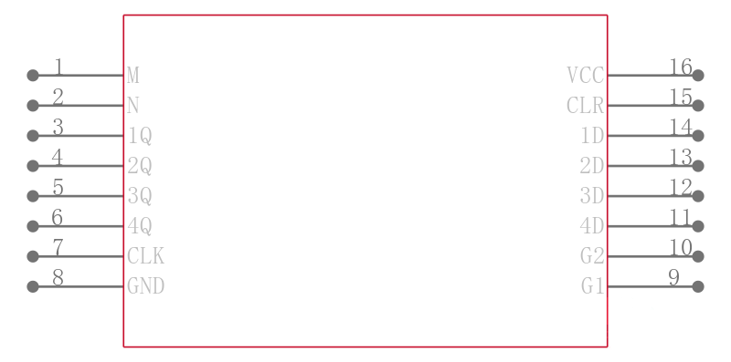
Gated enable inputs are provided on these devices for controlling the entry of data into the flip-flops. When both data-enable G\1, G\2 inputs are low, data at the D inputs are loaded into their respective flip-flops on the next positive transition of the buffered clock input. Gate output-control M, N inputs also are provided. When both are low, the normal logic states high or low levels of the four outputs are available for driving the loads or bus lines. The outputs are disabled independently from the level of the clock by a high logic level at either output-control input. The outputs then present a high impedance and neither load nor drive the bus line. Detailed operation is given in the function table.
The SN54173 and SN54LS173A are characterized for operation over the full military temperature range of -55°C to 125°C. The SN74173 and SN74LS173A are characterized for operation from 0°C to 70°C.
- .
- 3-State Outputs Interface Directly With System Bus
- .
- Gated Output-Control LInes for Enabling or Disabling the Outputs
- .
- Fully Independent Clock Virtually Eliminates Restrictions for Operating in One of Two Modes:
- .
- Parallel Load
- .
- Do Nothing Hold
- .
- For Application as Bus Buffer Registers
- .
- Package Options Include Plastic Small-Outline D Packages, Ceramic Flat W Packages, Ceramic Chip Carriers FK, and Standard Plastic N and Ceramic J DIPs
| 型号/品牌 | 代替类型 | 替代型号对比 |
|---|---|---|
SN74LS173A TI 德州仪器 | 当前型号 | 当前型号 |
SN54LS173A 德州仪器 | 功能相似 | SN74LS173A和SN54LS173A的区别 |