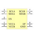
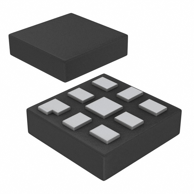
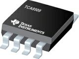

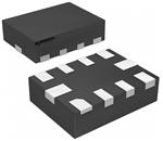
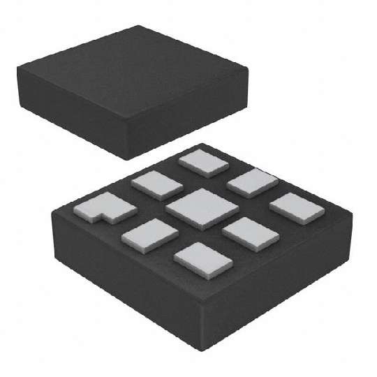

TEXAS INSTRUMENTS TCA9509RVHR 芯片, 总线中继器, I2C, 8X2QFN
This TCA9509 integrated circuit is an I2C bus/SMBus Repeater for use in I2C/SMBus systems. It can also provide bidirectional voltage-level translation up-translation/down-translation between low voltages down to 0.9 V and higher voltages 2.7 V to 5.5 V in mixed-mode applications. This device enables I2C and similar bus systems to be extended, without degradation of performance even during level shifting.
The TCA9509 buffers both the serial data SDA and the serial clock SCL signals on the I2C bus, thus allowing 400-pF bus capacitance on the B-side. This device can also be used to isolate two halves of a bus for voltage and capacitance.
The TCA9509 has two types of drivers A-side drivers and B-side drivers. All inputs and B-side I/Os are overvoltage tolerant to 5.5V. The A-side I/Os are overvoltage tolerant to 5.5V when the device is unpowered VCCB and/or VCCA=0V.
The bus port B drivers are compliant with SMBus I/O levels, while the A side uses a current sensing mechanism to detect the input or output LOW signal which prevents bus lock-up. The A side uses a 1 mA current source for pull-up and a 200 Ω pull-down driver. This results in a LOW on the A side accommodating smaller voltage swings. The output pull-down on the A side internal buffer LOW is set for approximately 0.2 V, while the input threshold of the internal buffer is set about 50 mV lower than that of the output voltage LOW. When the A side I/O is driven LOW internally, the LOW is not recognized as a LOW by the input. This prevents a lock-up condition from occurring. The output pull-down on the B side drives a hard LOW and the input level is set at 0.3 of SMBus or I2C-bus voltage level which enables B side to connect to any other I2C-bus devices or buffer.
The TCA9509 drivers are not enabled unless VCCA is above 0.8 V and VCCB is above 2.5 V. The enable EN pin can also be used to turn the drivers on and off under system control. Caution should be observed to only change the state of the EN pin when the bus is idle.
电源电压DC 2.70V ~ 5.50V
输出接口数 2
输出电流 6.00 mA
供电电流 3 mA
通道数 1
针脚数 8
耗散功率 100 mW
输入电容 6.5 pF
输入电容Ciss 7 pF
工作温度Max 85 ℃
工作温度Min -40 ℃
耗散功率Max 100 mW
电源电压 2.7V ~ 5.5V
电源电压Max 5.5 V
电源电压Min 2.7 V
安装方式 Surface Mount
引脚数 8
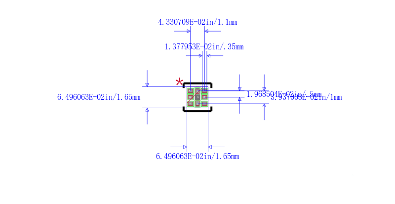
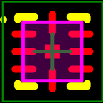
封装 XFQFN-8
封装 XFQFN-8
工作温度 -40℃ ~ 85℃
产品生命周期 Active
包装方式 Cut Tape CT
制造应用 I²C
RoHS标准 RoHS Compliant
含铅标准 Lead Free
REACH SVHC标准 No SVHC
REACH SVHC版本 2015/06/15
ECCN代码 EAR99