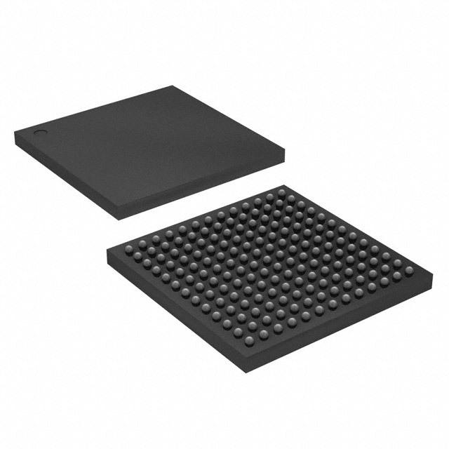
FPGA MAX 10 Family 16000 Cells 55nm Technology 3V/3.3V 169Pin UBGA
* RoHS6-compliant * 16 Logic Elements LE * Core architecture * LEs arranged in logic array block LAB * Embedded RAM and user flash memory * Clocks and PLLs * Embedded multiplier blocks * General purpose I/Os * User flash memory UFM * User accessible non Volatile storage * High speed operating frequency * Large memory size * High data retention * Multiple interface option * Embedded multiplier blocks * Cascadable blocks enabling creation of filters, arithmetic functions, and image processing pipelines * Clock networks * Global clocks support * High speed frequency in clock network * Configuration * Internal configuration * JTAG * Advanced Encryption Standard AES 128-bit encryption and compression options * Flash memory data retention of 20 years at 85°C