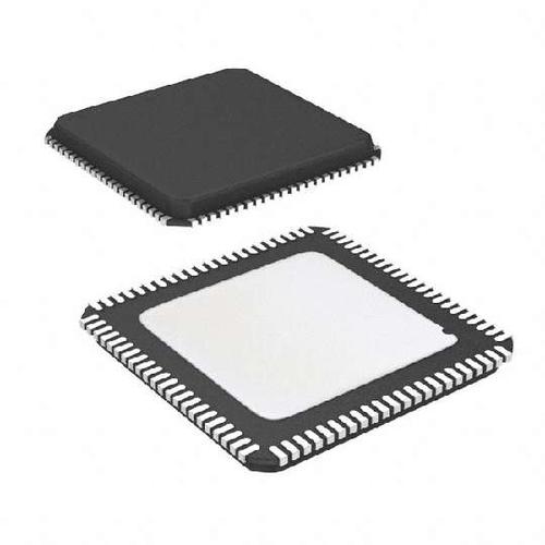
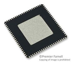
ANALOG DEVICES AD9531BCPZ 芯片, 时钟发生器, 3通道, 24路输出, LFCSP-88
Product Details
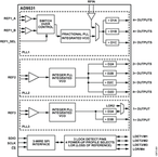
The AD9531 provides a multioutput clock generator function and three on-chip phase-locked loop PLL cores with SPI programmable output frequencies and formats.
PLL1 provides two reference inputs and 10 outputs and includes four user selectable loop configurations. The PLL has a fully integrated loop filter requiring only a single external capacitor or a series RC network. PLL1 provides a wide range of output frequencies up to 400 MHz and is capable of operating with an external voltage controlled crystal oscillator VCXO and loop filter, instead of the integrated voltage controlled oscillator VCO and loop filter.
PLL2 is an integer-N PLL providing a single reference input and 12 outputs. PLL2 synthesizes output frequencies up to 400 MHz from the REF2_x source and synchronizes the output clocks to the input reference.
PLL3 provides a single reference input and two outputs. PLL3 synthesizes output frequencies up to 400 MHz from the REF3_x source and synchronizes the output clocks to input reference.
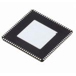
The AD9531 is available in an 88-lead LFCSP and is specified over the −40°C to +85°C operating temperature range.
Throughout this data sheet, multifunction pins, such as LOR/M4, are referred to either by the entire pin name or by a single function of the pin for example, LOR, when only that function is relevant. In other cases, the text and figures of this data sheet contain references to a channel rather than a pin. For example, REF_A refers to the REF_A channel rather than the REF_AP and REF_AN pins. Likewise, OUT3_1 refers to Channel 1 of PLL3 rather than the OUT3_1P and OUT3_1N pins. Additionally, an abbreviated notation for a pin pair replaces an explicit reference to a each pin for example, REF_Ax signifies the REF_AN and REF_AP pins..
**Applications**
- .
- Radio equipment controller clocking
- .
- Low jitter/phase noise clock generation and distribution
- .
- Clock generation and translation for SONET, 10GE, 10G FC, and other 10 Gbps protocols
- .
- 40 Gbps/100 Gbps networking line cards, including SONET, synchronous ethernet, OTU2/3/4
- .
- Forward error correction G.710
- .
- High performance wireless transceivers
- .
- ATE and high performance instrumentation
- .
- Broadband infrastructures
- .
- Ethernet line cards, switches, and routers
- .
- SATA and PCI-express
### Features and Benefits
- .
- 3 fully integrated PLL/VCO cores PLL1, PLL2, and PLL3
- .
- Jitter performance: 0.462 ps rms typical PLL1, fractional-N mode, 12 kHz to 20 MHz bandwidth
- .
- Loss of reference and lock detection for each PLL
- .
- Pin-configurable common frequency translations
- .
- Automatic synchronization of all outputs on power-up
- .
- Manual output synchronization capability
- .
- Package available in an 88-lead LFCSP
- .
- PLL1 details
- .
- Fractional-N/integer-N modes
- .
- Optional external VCXO
- .
- PLL2 details
- .
- Integer-N mode 1 reference clock input
- .
- Input format: differential/single-ended/crystal
- .
- PLL3 details
- .
- Integer-N mode 1 reference clock input
- .
- Frequency range: 9.5 MHz to 100 MHz
- .
- See data sheet for additional features
频率 400 MHz
电源电压DC 1.80V min
输出接口数 24
电路数 3
针脚数 88
占空比 60% Max
工作温度Max 85 ℃
工作温度Min -40 ℃
电源电压 1.71V ~ 3.465V
电源电压Max 3.3 V
电源电压Min 1.8 V
安装方式 Surface Mount
引脚数 88
封装 LFCSP-88
封装 LFCSP-88
工作温度 -40℃ ~ 85℃
产品生命周期 Active
包装方式 Tray
RoHS标准 RoHS Compliant
含铅标准 Lead Free
REACH SVHC版本 2015/12/17
ECCN代码 EAR99