

SILICON LABS芯科/C8051F060
System Overview
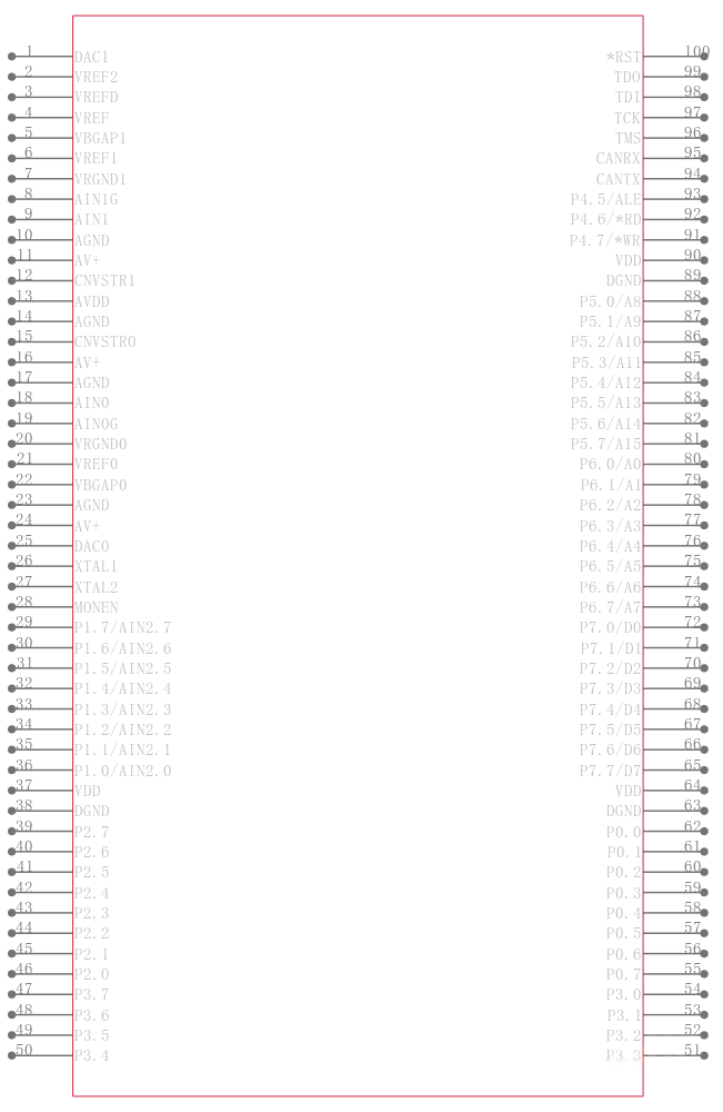
The C8051F06x family of devices are fully integrated mixed-signal System-on-a-Chip MCUs with 59 digital I/O pins /2/4/6 or 24 digital I/O pins C8051F061/3/5/7, and two integrated 16-bit 1 Msps ADCs. Highlighted features are listed below; refer to Table 1.1 for specific product feature selection.
• High-Speed pipelined 8051-compatible CIP-51 microcontroller core up to 25 MIPS
• Two 16-bit 1 Msps ADCs with a Direct Memory Access controller
• Controller Area Network CAN 2.0B Controller with 32 message objects, each with its own indentifier mask C8051F060/1/2/3
• In-system, full-speed, non-intrusive debug interface on-chip
• 10-bit 200 ksps ADC with PGA and 8-channel analog multiplexer C8051F060/1/2/3
• Two 12-bit DACs with programmable update scheduling C8051F060/1/2/3
• 64 kB C8051F060/1/2/3/4/5 or 32 kB C8051F066/7 of in-system programmable Flash memory
• 4352 4096 + 256 bytes of on-chip RAM
• External Data Memory Interface with 64 kB direct address space C8051F060/2/4/6
• SPI, SMBus/I2C, and 2 UART serial interfaces implemented in hardware
• Five general purpose 16-bit Timers
• Programmable Counter/Timer Array with six capture/compare modules
• On-chip Watchdog Timer, VDD Monitor, and Temperature Sensor
Analog Peripherals
\- Two 16-Bit SAR ADCs
• 16-bit resolution
• ±0.75 LSB INL, guaranteed no missing codes
• Programmable throughput up to 1 Msps
• Operate as two single-ended or one differential con verter
• Direct memory access; data stored in RAM without software overhead
• Data-dependent windowed interrupt generator
\- 10-bit SAR ADC C8051F060/1/2/3
• Programmable throughput up to 200 ksps
• 8 external inputs, single-ended or differential
• Built-in temperature sensor
\- Two 12-bit DACs C8051F060/1/2/3
• Can synchronize outputs to timers for jitter-free wave form generation
\- Three Analog Comparators
• Programmable hysteresis/response time
\- Voltage Reference
\- Precision VDD Monitor/Brown-Out Detector
On-Chip JTAG Debug & Boundary Scan
\- On-chip debug circuitry facilitates full-speed, nonintrusive in-circuit/in-system debugging
\- Provides breakpoints, single-stepping, watchpoints, stack monitor; inspect/modify memory and registers
\- Superior performance to emulation systems using ICE-chips, target pods, and sockets
\- IEEE1149.1 compliant boundary scan
\- Complete development kit
High Speed 8051 µC Core
\- Pipelined instruction architecture; executes 70% of instruction set in 1 or 2 system clocks
\- Up to 25 MIPS throughput with 25 MHz clock
\- Flexible Interrupt sources
Memory
\- 4352 Bytes internal data RAM 4 k + 256
\- 64 kB C8051F060/1/2/3/4/5, 32 kB C8051F066/7 Flash; In-system programmable in 512-byte sectors
\- External 64 kB data memory interface with multiplexed and non-multiplexed modes C8051F060/2/4/6
Digital Peripherals
\- 59 general purpose I/O pins C8051F060/2/4/6
\- 24 general purpose I/O pins C8051F061/3/5/7
\- Bosch Controller Area Network CAN 2.0B - C8051F060/1/2/3
\- Hardware SMBus™ I2C™ Compatible, SPI™, and two UART serial ports available concurrently
\- Programmable 16-bit counter/timer array with 6 capture/compare modules
\- 5 general purpose 16-bit counter/timers
\- Dedicated watchdog timer; bi-directional reset pin
Clock Sources
\- Internal calibrated precision oscillator: 24.5 MHz
\- External oscillator: Crystal, RC, C, or clock
Supply Voltage .......................... 2.7 to 3.6 V
\- Multiple power saving sleep and shutdown modes
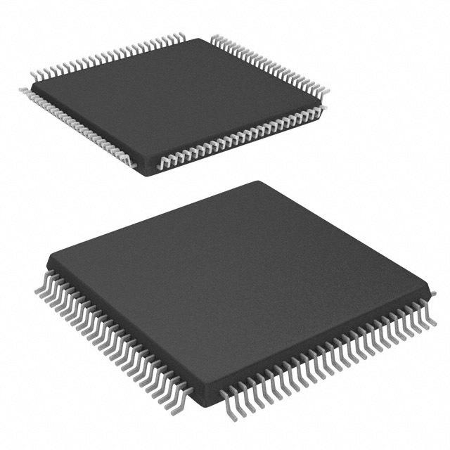
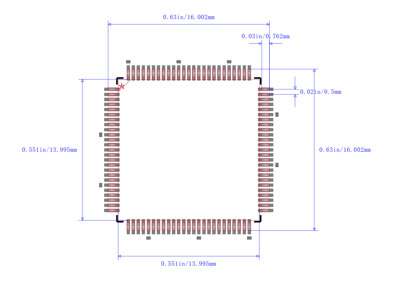
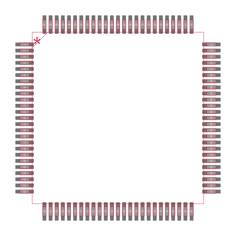
100-Pin and 64-Pin TQFP Packages Available Temperature Range: -40 to +85 °C
电源电压DC 3.30 V, 3.60 V max
工作电压 2.7V ~ 3.6V
通道数 6
时钟频率 25.0MHz max
RAM大小 4.25K x 8
FLASH内存容量 64000 B
I/O引脚数 59
存取时间 25.0 µs
内核架构 8051
工作温度Max 85 ℃
工作温度Min 40 ℃
电源电压Max 3.6 V
电源电压Min 2.7 V
安装方式 Surface Mount
引脚数 100
封装 TQFP-100
长度 14 mm
宽度 14 mm
高度 1 mm
封装 TQFP-100
工作温度 -40℃ ~ 85℃ TA
产品生命周期 Obsolete
包装方式 Tape & Reel TR
RoHS标准 Non-Compliant
含铅标准 Contains Lead
| 型号/品牌 | 代替类型 | 替代型号对比 |
|---|---|---|
C8051F060 Silicon Labs 芯科 | 当前型号 | 当前型号 |
C8051F060-GQ 芯科 | 类似代替 | C8051F060和C8051F060-GQ的区别 |